Implementation of an atmospheric muon telescope DAQ using the ARTY A7 FPGA developement board by Digilent.
- Software used for synthesis, implementation and bitstream generation: Vivado 2021.1
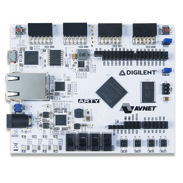
- Hardware used: Arty A7-35T evaluation board (Digilent): Artix 7 FPGA by Xilinx
- Hardware description language adopted: SystemVerilog and a little of VHDL (see below).
- Note: to build this project, since I needed to characterise the XADC, I have created another project containing the XADC which is sampling data from the analog pins and returns the sampled results via the UART cable on a terminal. Give a look to the repository Sampler XADC repository.
Now, it is possible to discuss the functionalities implemented on the designed device. In the digital circuit designed there are the following components:
-
An Analog-to-Digital converter in which the XADC core, provided by Xilinx, is included. A decoder is attached to this ADC in order to associate each analog pins on the board to its own address.
-
A digital signal processing pipeline manipulate the incoming data. At the beginning of the DSP pipeline there is a DC block filter which removes the DC component of the signal. Then, positive edged triggers, peak detectors, and area detectors are included in the design
- The peak detector is aimed to the collection of the maximum value of the incoming signal
- The area detector is aimed to the computation of the integral of the signal
-
Then, a data acquisition collects all the data coming from the DSP pipeline such as the peak-values, the area of the signals, the time of the event, and it has the task to unify all these pieces of information in some latches, ready to be acquired by the module which will send all these data through the UART cable.
-
A module called "Printer" is aimed to collect the data on a computer terminal. Inside this module there are FIFOs (from Xilinx IP catalogue), uart protocol module (from SystemVerilog book), and binary-to-BCD converters (this module is taken from the nanland website and it has been revisited a little).
In the figure below, it is possible to see the format of the data measured with this instrument. The reported example is made for only 2 analog channels. All the device, however, is parametrised, and, from the top module, one can easily add more channels to the design.

From left to right, referring to the previous figure we have:
- The time of the event expressed in millisecond (8 digits)
- The peak-value of the channel A0 (5 digits)
- The peak-value of the channel A1 (5 digits)
- The area-value detected for the signal on channel A0 (9 digits)
- The area-value detected for the signal on channel A1 (9 digits)
- The threshold (5 digits)
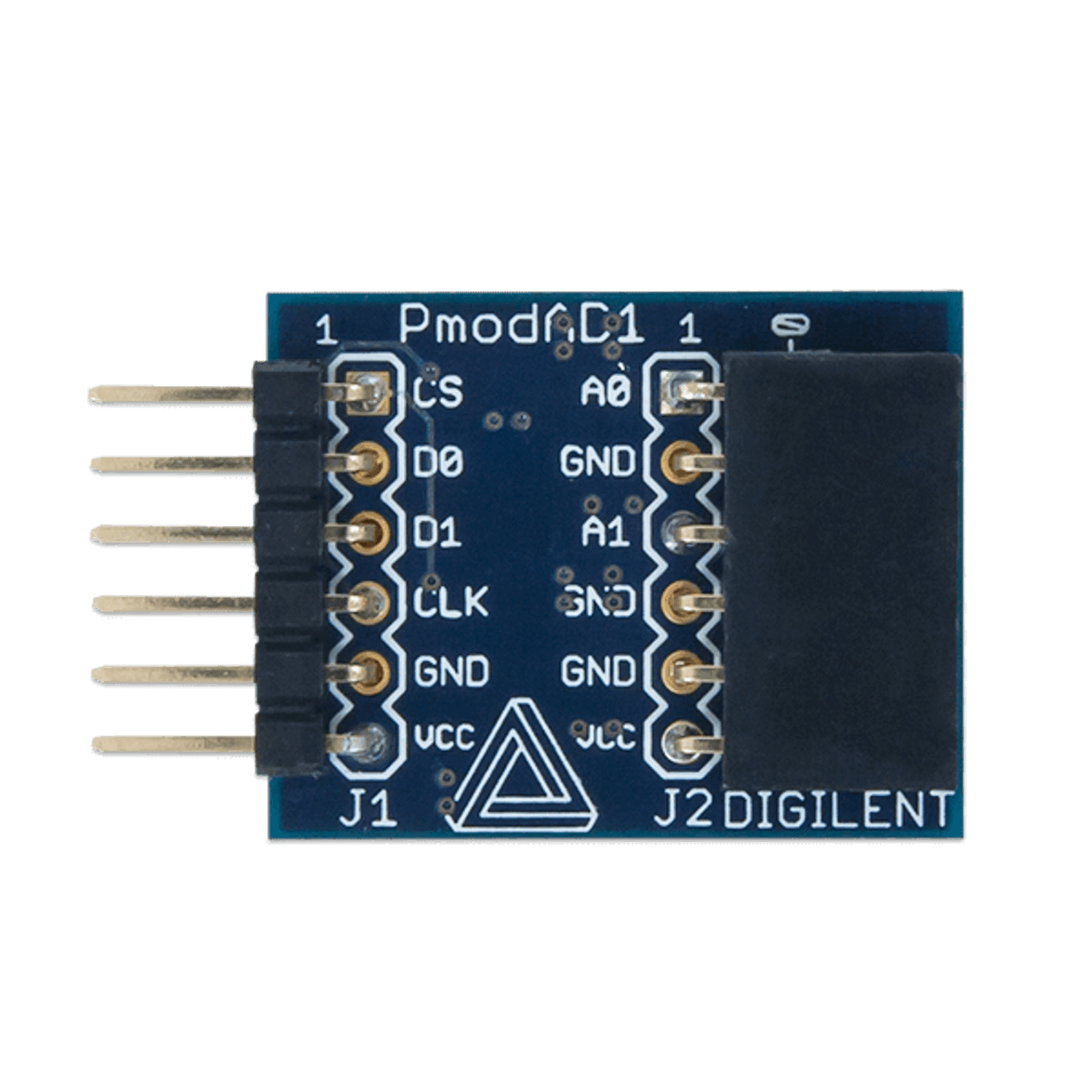
- 03/04/2021 Added two analog channels via the Pmod AD1 by Digilent. (see the Sampler PmodAD1 project)
The aim of this project is to develop a portable muon telescope using a relatively cheap FPGA developemente board, a tile of scintillating material and different SiPM. The concept behind this instrument is that a particle, hitting the scintillating material will release energy inside this emitting UV-visible photons. These visible photons are then absorbed by the Silicon PhotoMultipliers (SiPM) giving us a measurable voltage signal. The voltage signal is then digitalised by the XADC mounted on the Arty A7-35T developement board. The FPGA is then used for the data acquisition and data processing.
Below it is reported the structure of the directory
.
├── Darticle-Detector-ARTY-A7
│   ├── Darticle-Detector-ARTY-A7.cache
│   ├── Darticle-Detector-ARTY-A7.hw
│   ├── Darticle-Detector-ARTY-A7.ip_user_files
│   ├── Darticle-Detector-ARTY-A7.runs
│   ├── Darticle-Detector-ARTY-A7.sim
│   └── Darticle-Detector-ARTY-A7.xpr
├── docs
│   └── assets
├── Firmware-SRC
│   ├── adc_demux.sv
│   ├── baud_gen.sv
│   ├── binary_BCD.sv
│   ├── Buffers_reg.sv
│   ├── DAQ.sv
│   ├── db_fsm.sv
│   ├── DC_blocker.sv
│   ├── debouncing_array.sv
│   ├── DSP_pipeline.sv
│   ├── fifo_generator_area
│   ├── fifo_generator_peak
│   ├── fifo_generator_time
│   ├── fifo_generator_uart
│   ├── Frequency_Divider.sv
│   ├── left_padding.sv
│   ├── Monostable_rise_only.sv
│   ├── Monostable.sv
│   ├── muon_telescope_top.sv
│   ├── Peak_detector.sv
│   ├── pmod_wrapper.vhd
│   ├── Printer_uart.sv
│   ├── SPI_master_dual_miso.vhd
│   ├── SynchroCounter_4_bit.sv
│   ├── test_unit.sv
│   ├── threshold_controller.sv
│   ├── time_measurement.sv
│   ├── Trigger.sv
│   ├── uart_rx.sv
│   ├── uart.sv
│   ├── uart_tx.sv
│   ├── XADC_module.sv
│   └── xadc__netlist.v
├── Firmware-TB
│   ├── Data_acquisition_tb.sv
│   ├── DSP_pipeline_tb.sv
│   ├── my_testbench_tb.sv
│   ├── tb_peak_area_detector.sv
│   ├── threshold_contr_tb.sv
│   └── trigger_tb.sv
├── Firmware-XDC
│   └── Arty-A7-35-Master.xdc
└── README.md
- In the directory
Firmware-SRCyou'll find all the modules of the firmware. Modules are written using SystemVerilog which is a superset of Verilog HDL. This hardware description language is very similar to Verilg but it allows parametrisation of the modules - In the directory
Firmware-TByou'll find all the testbenches I used for testing and debugging the modules in the design. They are written in SystemVerilog and the simulation of the modules can be carried out with Vivado - The directory
Firmware-XDCcontains the costraints to be used for the ARTY A7 development board
All the folders inside this repository are automatically generated by Vivado. However, it is useful to know how to read them and how to build up a working project using the Vivado software.
This repository contains the following folders:
_PROJECT_NAME_.hw: In this folder are contained the information about the eventual exported hardware._PROJECT_NAME_.srcs: This is the folder containing all the sources files added to the project. The SystemVerilog files are at the following link
- SystemVerilog files
- Costraint file (.xdc): The costraint files for all the Digilent boards can be found at the following link Digilent/digilent-xdc.
To build up a Vivado project, the following operations are required:
- Open Vivado
- Click on New project
- Give a name to the project and click on Create project subdirectory and click on Next
- Click on RTL project. Then, click Next
- Now choose all the sources files .v (if the files are written in verilog), .sv (if they are written in SystemVerilog), .vhd (if files are written in VHDL), click on Scan and add RTL include files into the project and Copy sources into project. Then, click on Next
- Import the Costraint file .xdc in the same manner as before.
- Now you need to select the Target device. To do this, select the Boards menu and search for ARTY A7-35T. To do this operation you need to install on your computer the Digilent boards files. This procedure is described at the following link https://digilent.com/reference/programmable-logic/guides/installing-vivado-and-vitis if you use the latest versions of Vivado and Vitis unified platform or the following link https://digilent.com/reference/programmable-logic/guides/installing-vivado-and-sdk if you use Vivado and Vivado SDK.
- Now it is possible to modify the project, run the synthesis, the implementation and the bitstream generation
For more information give a look to the tutorial Getting started with Vivado on the Digilent website.
Other tutorials at the following links:
To add more analog channels to our device, it has been used the Pmod AD1 by Digilent
The PmodAD1 contains a pair of AD7476A ADCs by Analog Devices
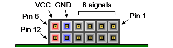
Let's see the configuration for the pins on the board.
Below is reported the schematic of the Pmod interface.
I have used the JC interface since it is configured to run at High-speeds.
| Pin figure | Pin XDC (vector) | Pin FPGA | Pmod connection | Direction |
|---|---|---|---|---|
| 1 | 0 | U12 | Not used | -- |
| 2 | 1 | V12 | Not used | -- |
| 3 | 2 | V10 | Not used | -- |
| 4 | 3 | V11 | Not used | -- |
| 7 | 4 | U14 | CS negation | Output |
| 8 | 5 | V14 | D0 (MISO) | Input |
| 9 | 6 | T13 | D1 (MISO) | Input |
| 10 | 7 | U13 | CLK | Output |
Note :
- Input : from the external Pmod towards the FPGA
- Output : from the FPGA towards the external device
The core containing the SPI interface to collect data from the PmodAD1 can be found at the following website Digi-Key link. The core is written in VHDL. Vivado, the tool provided by Xilinx, allow the language mixing within a project. Hence, using the traditional Verilog instantiation template, it is possible to use the VHDL core.
Here some particular pieces of information about the project:
-
The Device has been developed using SystemVerilog HDL
-
The top module is "muon_telescope_top_module" and inside the module definition there are some parameters which have to be set up correctly by the user before synthesis to chosing the number of acquired channels
-
The system is clocked using the mounted 100 MHz clock.
-
The system reset is the button C2. However, this is active high. It has been generated an active low reset to prevent misunderstanding in the design.
-
To avoid bouncing effects from the push buttons, some debouncers are placed into the design.
-
Switches are used to setup the increment of the threshold controller.
This solution is not preatty elegant but it is one possible way I found for the solution of the problem of changing the number of channels of the XADC.
If you change the number of channels in the top module, then you need to open the "XADC Wiziard" in Vivado software, change the "Sequenced channels" and re-run the synthesis of the component XADC. When the synthesis is finished you need to open the file "NAME_stub.v" in the IP resources, copy the code
      .INIT_40(16'h0000),
      .INIT_41(16'h21A0),
      .INIT_42(16'h0400),
      ...
and replace the part contained in the file "NAME_netlist.v". This is required because the XADC module comes from an IP by Xilinx and to set up properly the sequencer settings you need to generate the encrypted sources. In principle one could change by hand the registers in the instantiation (.INIT_40(1b'h...)). This procedure, however, is quite tedious since it is required to know the meaning of all these registers. The procedure exploiting the XADC wiziard is more "user friendly" even if it is a bit longer. After generating the correct template for the XADC module you need to "disable the source file" using the Vivado navigation menu. This because in the xadc_netlist.v file there are the instructions used by vivado to generate the required sources and so the IP generated via the IP catalogue is unnecessary.
The project is not yet finished and probably there are some errors in the code :P
- Digilent reference webpage (Arty A7) : https://digilent.com/reference/programmable-logic/arty-a7/start
- Arty A7 reference manual : https://digilent.com/reference/programmable-logic/arty-a7/reference-manual
- OpenCores (a useful web platform where it is possible to find HDL open source cores) : https://opencores.org/
- Companion website for the book FPGA prototyping by SystemVerilog examples by Dr. Chu : https://academic.csuohio.edu/chu_p/index.html
- Xilinx Vivado website: https://www.xilinx.com/products/design-tools/vivado.html
- Digilent GitHub repositories : https://github.com/digilent
- Xilinx Github repository: https://github.com/Xilinx