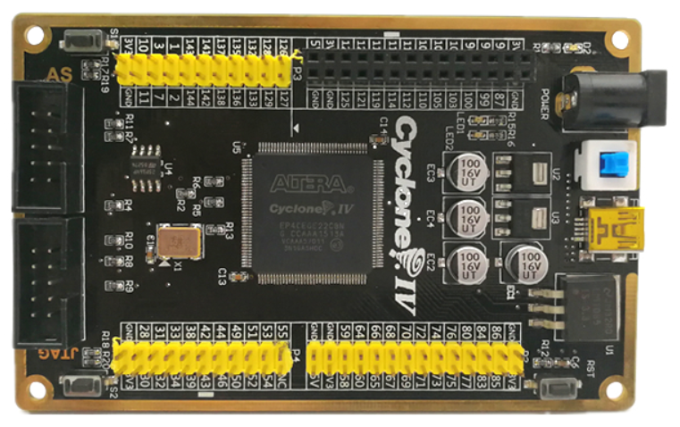
These are a collection of notes and resources, inasmuch for myself as for anyone else who might need it. They are a combination of what the seller has sent to me (i.e., schematics) and information I have gleamed from probing the board myself while referring to the schematics. If you find any errors, please let me know, or fork and make a pull request. NO WARRANTY IS PROVIDED, either expressed or implied. As always, the best is to double check yourself before you do something irreversible.
NB!!! Make sure you ONLY POWER THE BOARD WITH 5V DC at the DC barrel jack, or with a USB cable
This is as close as I can figure them out to be. While the ports may have fixed "purposes" when combined with the seller's ready-made expansion modules, as-is, they can be considered to be general purpose I/O as well.
| Port Name/Label | Usage |
|---|---|
| Power | Provide DC 5V 1A power to the board |
| Blue switch | Turns DC barrel jack power on/off |
| USB Type B Mini | Power the board with USB. No data |
| P1 header | For camera module or General Purpose |
| P2 header | For VGA/SD Card/PS2/Ethernet module(s) |
| P3 header | For SDRAM module or General Purpose |
| P4 header | For SDRAM module or General Purpose |
| AS IDC port | "Active Serial" - To directly program the SPI config memory |
| JTAG IDC port | For JTAG programming |
Only the unlabelled pin assignments will be indicated here - as for the pin headers themselves, the package pin numbers are already printed next to the pins themselves so I would direct you to either the schematic or the board silkscreen itself for reference.
| Signal Name | Pin Number | Notes |
|---|---|---|
| LED1 | 98 | Logic 0 to turn on. |
| LED2 | 87 | Logic 0 to turn on. |
| S1 | 24 | Pull-Up resistor |
| S2 | 25 | Pull-Up resistor |
| CLOCK (X1) | 23 | 50 MHz |
| RESET | 88 | Active low |
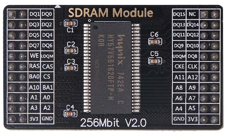
An SDRAM module is available that fits the P3 and P4 headers exactly, with the top left corner being indicated with an alignment arrow on both the Core board and the SDRAM module. The module features a 256Mbit (32MB) Hynix HY57V561620FTP-H SDRAM chip in a 400 mil 54-pin TSSOP II package.
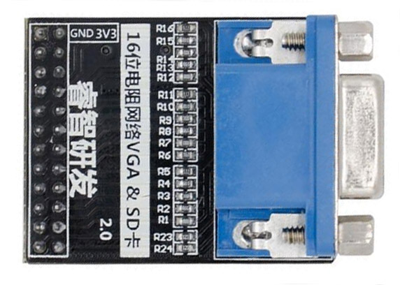
The VGA and Micro SD-Card Module is meant to be plugged into header P2, being sure to align the GND and 3V3 (3.3V) pins which are marked on the module itself. The VGA pinout uses a resistor ladder connected to a 16-bit RGB output formatted in the popular 5-6-5 bitfield arrangement. The Micro SD Card connector is wired up in SPI mode.
| FPGA Pin | Function | Function | FPGA Pin | ||
|---|---|---|---|---|---|
| GND | 1 | 2 | 3V3 | ||
| 86 | SD-MOSI | 3 | 4 | SD-CS | 85 |
| 84 | SD-MISO | 5 | 6 | SD-CLK | 83 |
| 80 | Red | 7 | 8 | Red | 77 |
| 76 | Red | 9 | 10 | Red | 75 |
| 74 | Red | 11 | 12 | Green | 73 |
| 72 | Green | 13 | 14 | Green | 71 |
| 70 | Green | 15 | 16 | Green | 69 |
| 68 | Green | 17 | 18 | Blue | 67 |
| 66 | Blue | 19 | 20 | Blue | 65 |
| 64 | Blue | 21 | 22 | Blue | 60 |
| 59 | VSYNC | 23 | 24 | HSYNC | 58 |


