
Shielded loop probes have a variety of uses in RF engineering, including as "sniffer" probes for electromagnetic (EM) compatibility (EMC) or interference (EMI) measurements in conjunction with a spectrum analyzer. They are also used to measure the H fields of resonant or radiating structures (antennas). In MRI and NMR they are connected to a network analyzer (VNA) to measure the frequency response of RF detector "coils", e.g., to ensure tuning at the Larmor frequency.
The shielded loop was originally described for use as an antenna by RE Burgess in “The Screened Loop Aerial: A Theoretical and Experimental Investigation”, The Wireless Engineer 16 (October 1939): 492–99.
Shielded loop probes are designed to pick up magnetic (H) fields using Faraday's law of induction. They are untuned (nonresonant) and have broadband response from a few kHz to several GHz. Output voltage is measured at the probe's terminals which is typically a coaxial connector (e.g., SMA or BNC).
Most of the loop is shielded to minimize sensitivity to electric (E) fields that are often present in addition to the H field. A small gap prevents the shield from shorting the voltage produced by the H field. It is preferable to place the gap in the centre of the loop to maintain symmetry, which ensures that the response will be unchanged if the probe is rotated by 180°.
Shielded loop probes are often made by hand on the RF workbench using semi-rigid, hand-formable or flexible coaxial cable. Photos, drawings and additional references are found in numerous sites online like https://www.uniteng.com/neildocs/references/Probing_the_Magnetic_Field_Probe.htm
Making loop probes using coax requires some skill and for small diameters it can be challenging. Reliability of the probe can also be an issue because solder joints can fail, and thin coax, even if semi-rigid, can bend quite easily. The probe described here uses a stripline printed inside a circuit board (4-layer 1.6 mm FR4 PCB), making it much more rugged and rigid than coax. Connection from the board to coaxial cable is made through a side-launch connector such as the SMA connector shown in the photos below.
A similar design is presented in this article: https://www.mdpi.com/2079-9292/10/18/2201
-
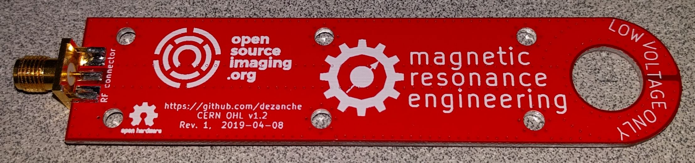
The first release (1.0) measures 23mm wide and ~100mm in length. The diameter of the loop is approximately 18mm with a central hole about 11mm ⌀. The panelized version allows 4 identical probes to be printed on a 100mm × 100mm panel (was used because of cost savings from a specific board house). Copies of this board were distributed at the 2019 annual scientific meeting of the ISMRM (Montreal). This design has a minor flaw: the whole board is covered by ground which can cause perturbation of fields throughout the length of the probe. In many cases the effect will be negligible, but for uses like near field mapping, or accurate measurement of resonance frequency this might be a concern.
-
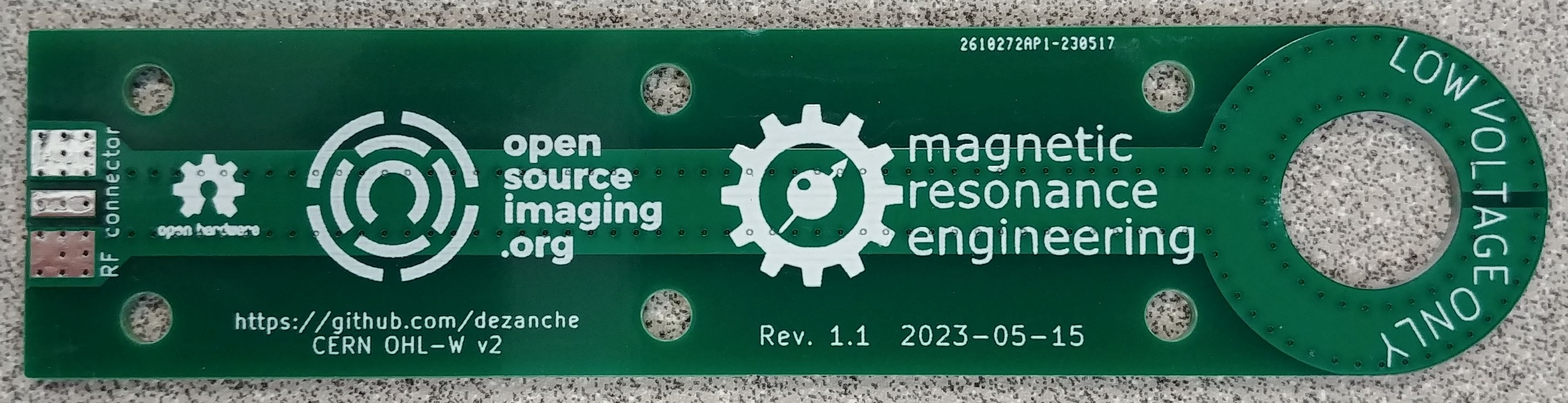
The second release (2.0) has identical measurements to the previous release and corrects the design flaw by using smaller ground planes. Copies of this board were distributed at the 2023 annual scientific meeting of the ISMRM (Toronto).


Lately, probes such as these have become inexpensive and available from various sources online, so it is unlikely that further revisions of this single-loop design will be made.
Nicola De Zanche
Layouts and other CAD files are licensed under the CERN-OHL-W 2.0 license, version 2.0 or any later version.
All other original content in this repository (including this README file) is licensed under a Creative Commons Attribution-NoDerivatives 4.0 International License.
