Questions? Try the Pano Logic gitter chat room! https://gitter.im/panologic/community
The project log can be found here.
This project starts with the work of The Cranky Sysadmin, and will build on top of that:
- In Search of FPGAs or Pano Logic Generation 1 Teardown
- Exploiting the FPGA in the Pano Logic Zero Client
- More Reverse Engineering of the Pano Logic Thin Client G1
- Pano Man implements the original PacMan on Pano G1
- There exists a low profile version of the Pano Logic G1 which seems to behave the same as the regular cube.
The pin constraint file can be found here.
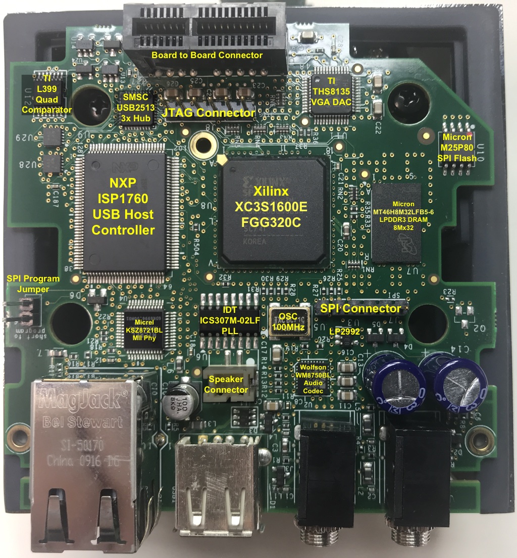
6 pin connector J8 is the JTAG connector. When the IO connectors are at the bottom, J8 is located at the top left of the Xilinx chip, and pin 1 is the one on the left.
The pin order does NOT follow the one of my Digilent clone.
Pinout is as follows:
- VCC
- TDI
- TMS
- TDO
- TCK
- GND
- GND
- CS#
- DQ1 (MISO)
- CLK
- DQ0 (MOSI)
- VCC
The SPI pins are used to configure the bitstream at power-up. After that, they become user IO.
To program the SPI, use the "Short to Program" jumper and attach SPI programmer to the connector. The "Short to Program" jumper pulls the PROG_B pin of the FPGA to ground, which forces all FPGA IOs into Hi-Z.
During development, since the JTAG is already connected anyway, it's easier to program the SPI flash through JTAG.
The procedure is simply: Using Impact, create an 'mcs' file that contains the bitstream in SPI programming format. Then use Impact to program that file into the SPI flash through JTAG.
Detailed instructions are here:
- Xilinx - Introduction to Indirect Programming – SPI or BPI Flash Memory
- Xilinx - Programming an SPI or BPI Flash Memory through an FPGA
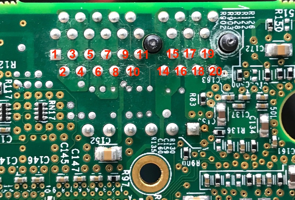
A* = inward facing side of the connector
A'* = outward facing side of the connector
| Pin | Function | FPGA | Misc |
|---|---|---|---|
| A1 | GND | ||
| A2 | VGA SCL | D4 | |
| A3 | GND | ||
| A4 | VGA SDA | G3 | |
| A5 | GND | ||
| A6 | VGA B analog | ||
| A7 | GND | ||
| A8 | VGA G analog | ||
| A9 | VGA VSYNC | D1 | |
| A10 | VGA R analog | ||
| A11 | VGA HSYNC | C2 | |
| A14 | GND | ||
| A15 | SMSC USB2513 USBDN2_DP pin 4 | ||
| A16 | SMSC USB2513 USBDN2_DM pin 3 | ||
| A17 | GND | ||
| A18 | SMSC USB2513 USBDN3_DM pin 6 | E5 | |
| A19 | SMSC USB2513 USBDN3_DP pin 7 | ||
| A20 | GND | ||
| A'1 | GND | ||
| A'2 | FPGA VCCO 3.3V | F3, K1, H7, ... | |
| A'3 | GND | ||
| A'4 | ? | 1.8V | |
| A'5 | GND | ||
| A'6 | VGA PWR (5V) | ||
| A'7 | GND | ||
| A'8 | Button | R7 | (Pressed is 3.3V) |
| A'9 | LED Green | H1 | |
| A'10 | LED Blue | L1 | |
| A'11 | LED Red | L3 | 4.8V (but 3.3V at FPGA) |
| A'14 | GND | ||
| A'15 | ? | 3.1V | |
| A'16 | ? | B7 | 2.45V |
| A'17 | GND | ||
| A'18 | ? | 1.2V | |
| A'19 | ? | 2.75V | |
| A'20 | GND |
Notes:
- VGA/SDA: Connected to top right pin of U23
- VGA/SCL: Connected to bottom right pin of U23
- U23: level shifters?
-
1600K system gates, 231K distribute RAM bits, 648K block RAM bits, 36 18x18 multipliers.
Supported by Xilinx ISE 14.7 Free edition! (Download here)
Full component name: XC3S1600E-FGG320 320 package. (Drawing) Speed grade 5, Commercial.
Ordering code: XC3S1600E-5-FGG320C
FG320 footprint is on page 208 of DS312.
Available at Digikey
Useful Guides:
-
Micrel KSZ8721BL 10/100BASE-TX/FX Ethernet MII Physical Layer Transceiver
10/100BASE-TX/FX MII Physical Layer Transceiver
Information regarding Ethernet has been gathered here
-
Codec with Speaker Driver
The control interface is configured to I2C (2-wire) mode, with the 8-bit address set to 0x34.
-
Programmable clock source
-
Hi-Speed Universal Serial Bus host controller for embedded applications with a built-in 3-port HUB. To mitigate one of the controller’s errata a separate 3-port HUB was installed on the board, only exposing one of the hub ports on the ISP1760 through the separate hub SMSC USB2513.
-
USB 2.0 High-Speed 3-Port Hub Controller
All 3 USB ports are connect to this controller.
-
Serial Flash Embedded Memory, 8Mbit.
A non-compressed XC3S1600E bitstream needs 5,969,696 bits (UG332, Table 1-4), which leaves ~2Mbit (512KByte) free for other uses.
It should be possible to replace the M25P80 with a larger version, such as the 16Mbit M25P16. These parts are end-of-life and not available anymore on Mouser or Digikey, but Adesto Tech makes compatible replacements.
Useful guides:
-
10-BIT 240-MSPS VIDEO DAC
Chip operates in general DAC mode. No analog SYNC pulses are generated because HSYNC and VSYNC are separate digital signals for VGA.
-
Micron Mobile Low-Power DDR SDRAM MT46H8M32LFB5-6
Chip has 'D9FSD' marker, which is the FPBA code for MT46H8M32LFB5-6:A.
2 Meg x 32 x 4 Banks = 8M x 32-bits or 32MByte.
166MHz clock. Max BW: 2 x 166 x 32 = 10.6 Gbit/s or 1.32 GByte/s. (24bpp 1080p@60 ~ 3Gbps)
The Xilinx ISE MIG tool only supports 8x and 16x regular DDR, not 32x LPDDR. So it looks like a custom DDR controller must be used for that?
Information regarding DDR has been gathered here.
-
Includes JTAG pin connector layout

