This repository provides a comprehensive characterization of a 7nm FinFET-based inverter designed using the ASAP7 PDK. The project includes schematic capture with Xschem, layout design using Magic, and simulation using NGSpice. The key deliverables are the DC, AC, and Voltage Transfer Characteristics (VTC) analysis, offering valuable insights into the performance of FinFET-based inverters at advanced technology nodes. This work is intended to serve as a resource for researchers, students, and engineers in the field of VLSI design and nanoelectronics. Contributions and feedback are welcome.
1. ASAP7 PDK
Description: The ASAP7 Process Design Kit (PDK) is a 7nm predictive PDK developed for academic use. It is based on FinFET technology and provides models, libraries, and design rules for advanced semiconductor design. The PDK is designed to give realistic simulation results for circuits operating in the sub-10nm regime, using predictive technology models.
Why Chosen: ASAP7 was selected for this project to accurately model and simulate 7nm FinFET-based designs. As the focus of the project is on next-generation semiconductor technology, ASAP7 provides the necessary tools and libraries to design, simulate, and validate FinFET-based circuits. This PDK helps ensure that the design matches real-world manufacturing conditions, with accurate parasitic, timing, and power estimates.
Version r1p7
2. BSIM4 CMG FinFET Model
Description: The BSIM4 Compact Multi-Gate (CMG) Model is a widely accepted SPICE model used for FinFET transistors. It offers a framework for simulating devices with multi-gate structures, including double-gate and triple-gate FinFETs, which are the foundation of modern nanometer-scale transistor technology.
Why Chosen: The BSIM4 CMG model was chosen due to its compatibility with FinFET technology, particularly the 7nm FinFETs used in this project. It provides a highly accurate representation of the electrical behavior of FinFET devices, including short-channel effects, mobility degradation, and quantum effects. This model is essential for achieving precise simulation results in advanced CMOS designs like the inverter being characterized.
3. OpenVAF
Description: OpenVAF (Open Verilog Analog Framework) is a tool used to integrate analog and mixed-signal simulations into a Verilog environment. It allows for both analog and digital simulations to coexist, enabling the simulation of circuits that involve both types of signals, such as inverters and mixed-signal systems.
Why Chosen: OpenVAF is used to bridge the gap between analog and digital simulations in this project. Given that the inverter design involves both analog characteristics (e.g., voltage transfer curves) and digital characteristics (e.g., logic levels), OpenVAF facilitates a seamless simulation workflow. It also allows for mixed-mode verification, ensuring the design is fully validated in both analog and digital domains.
Usage OpenVAF is used to generate the BSIM_OSDI Image compatible with NGSpice Simulation from the downloaded BSIM CMG Models
The bsimosdi.osdi file plays a crucial role when working with OpenVAF and BSIM4 CMG models in NGSpice simulations.
bsimosdi.osdi is a data file generated by OpenVAF that serves as an Optimized Simulator Sata Interface (OSDI) for BSIM models, specifically BSIM4 CMG FinFET models. This file encapsulates the device model information in a format that is highly efficient for NGSpice simulations, reducing the computational load required to handle complex FinFET device physics.
-
Download the BSIM CMG Model Files:
- These are provided by various sources (like Berkeley) for FinFET devices.
-
Generate the
bsimosdi.osdiFile Using OpenVAF:- OpenVAF processes the BSIM4 CMG model files and converts them into the
bsimosdi.osdiformat, which is optimized for NGSpice. - During this process, the model parameters are encoded into a format that NGSpice can directly interpret.
- OpenVAF processes the BSIM4 CMG model files and converts them into the
-
Include the
bsimosdi.osdiin NGSpice Simulations:- In your NGSpice simulation script (SPICE netlist), the
bsimosdi.osdifile is referenced to load the pre-compiled BSIM model data. - Symbol files are created using ASAP7 PDK Data for parameter values of BSIM CMG Model.
- These symbol files contain the reference for the generated
bsimosdi.osdiary file. - Example: In the 7nm NFET Symbol file
.control pre_osdi <path_to_generated_bsimosdi.osdi> .endc- NGSpice uses this osdi file to simulate the behavior of the FinFET devices in your circuit without needing to recalculate model parameters from scratch.
- In your NGSpice simulation script (SPICE netlist), the
4. Xschem
Description: Xschem is a graphical schematic editor used to design and capture analog, digital, and mixed-mode circuits. It supports hierarchical design, and its integration with NGSpice makes it a powerful tool for simulation and analysis. It’s particularly useful for creating circuit schematics and generating the necessary SPICE netlists for simulation.
Why Chosen: Xschem was chosen due to its user-friendly interface and seamless integration with NGSpice. For this project, where FinFET-based circuits like NFETs and inverters are being simulated, Xschem simplifies the design process and provides a quick way to visualize circuit schematics. Its support for hierarchical designs also helps in managing complex designs efficiently.
5. NGSpice
Description: NGSpice is an open-source mixed-level/mixed-signal electronic circuit simulator. It’s used for simulating circuits at the transistor level, offering SPICE-like capabilities. NGSpice is widely used in academic and professional settings to perform various types of simulations, including DC, AC, transient, and noise analysis.
Why Chosen: NGSpice was selected because of its powerful simulation capabilities, particularly for the DC and AC characterization of circuits in this project. It is essential for generating the voltage transfer characteristics (VTC) of the inverter design, and its compatibility with both Xschem and the BSIM4 CMG FinFET model makes it the ideal simulation tool for this FinFET-based project.
For further information, refer the Ngspice Manual
Types of Simulations
- DC Simulation: This is time-independent and is used to analyze circuits without considering time-varying elements like capacitors or inductors. Capacitors are treated as open circuits, and inductors as short circuits. This is useful for determining how circuits respond to fixed voltage or current sources.
- Transient Simulation: Time-dependent simulation, which models the behavior of circuits over time. It's more complex than DC simulations and requires initial conditions (often obtained from a preceding DC simulation) for capacitors and inductors.
- AC Simulation: Involves frequency-dependent analysis. It’s typically used for analog circuits like amplifiers, where you need to know the frequency range in which the amplifier works effectively.
1. Schematic Design
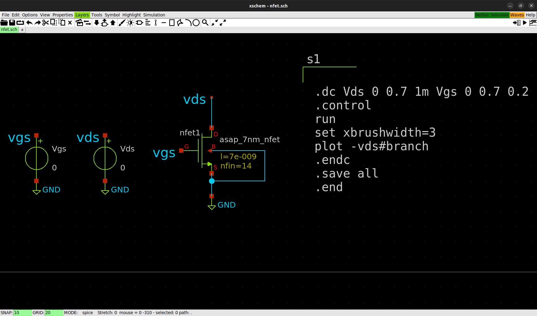
- The schematic design for the NFET was created in Xschem using the ASAP7 7nm FinFET library. The NFET is characterized with a gate voltage (Vgs) and drain voltage (Vds) to observe its electrical behavior.
- The NFET device has the following properties:
- Length (l): 7nm
- Number of fins (nfin): 14
- Voltage sources Vgs and Vds are applied, and the output characteristics are plotted.
2. Simulation Setup
- The NGSpice simulation runs a DC sweep for both Vds and Vgs to analyze the NFET behavior.
- The DC sweep is configured as:
.dc Vds 0 0.7 1m Vgs 0 0.7 0.2 - The simulation outputs the drain current (Id) as a function of the applied Vds and Vgs, providing insight into the transistor's switching behavior and current flow characteristics.
Simulation Parameters:
- Vds Sweep Range: 0V to 0.7V
- Vgs Sweep Range: 0V to 0.7V with a step of 0.2V
3. Simulation Results
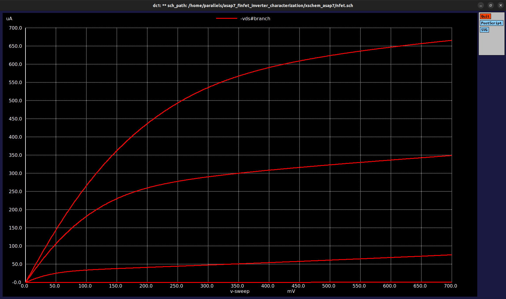
- The results include the Id vs Vds curve for different values of Vgs, showing how the drain current changes with increasing drain-source voltage for various gate-source voltages.
- This helps in understanding the linear and saturation regions of the NFET's operation.
1. Schematic Design
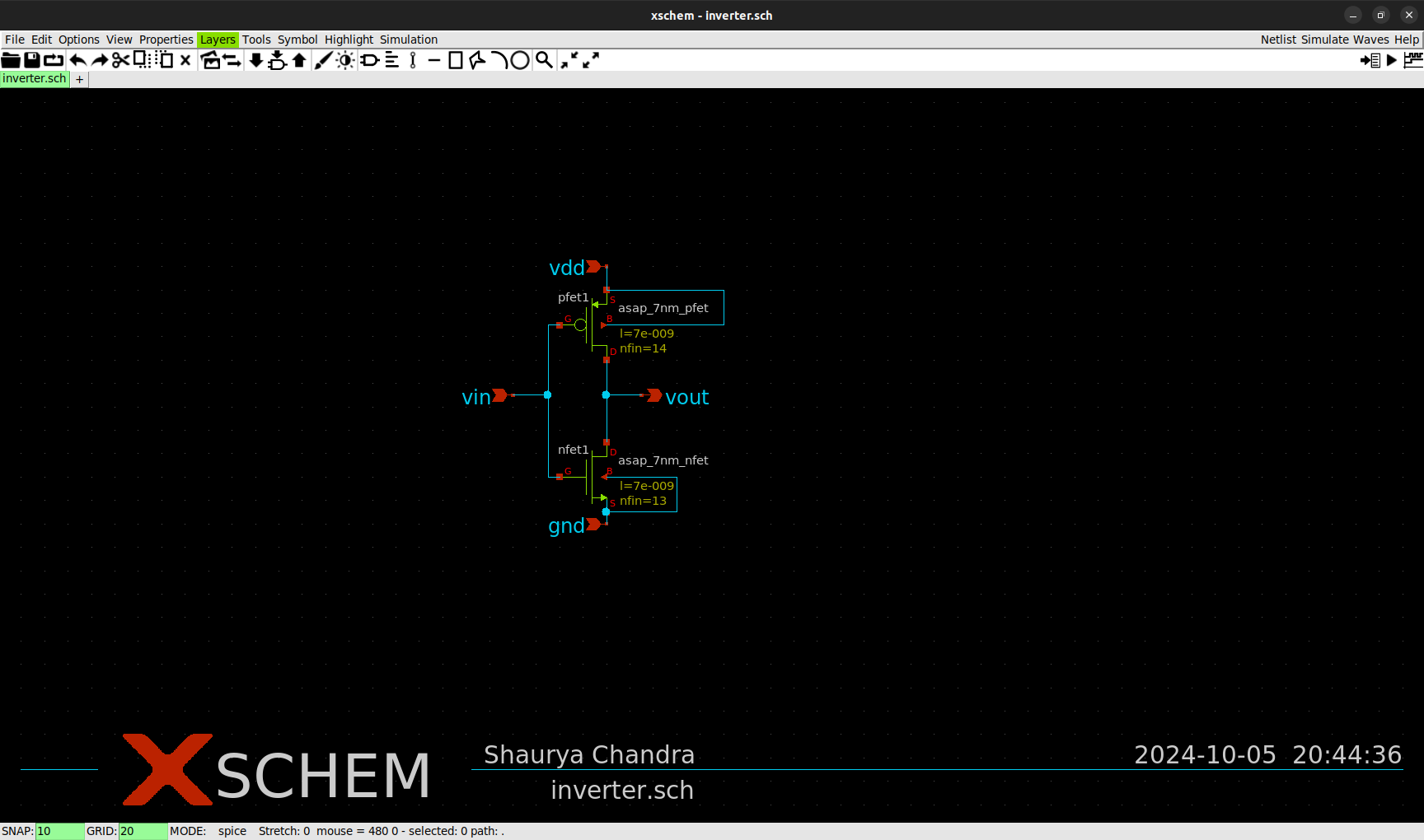
- The pre-layout schematic design of the inverter is created using Xschem. The design consists of a basic CMOS inverter with a PFET and NFET transistor, where the PFET is connected to VDD and the NFET to GND.
- The input signal, Vin, is applied to the gate terminals of both transistors, while the output signal, Vout, is observed at the shared drain of the PFET and NFET.
3. Inverter Testbench
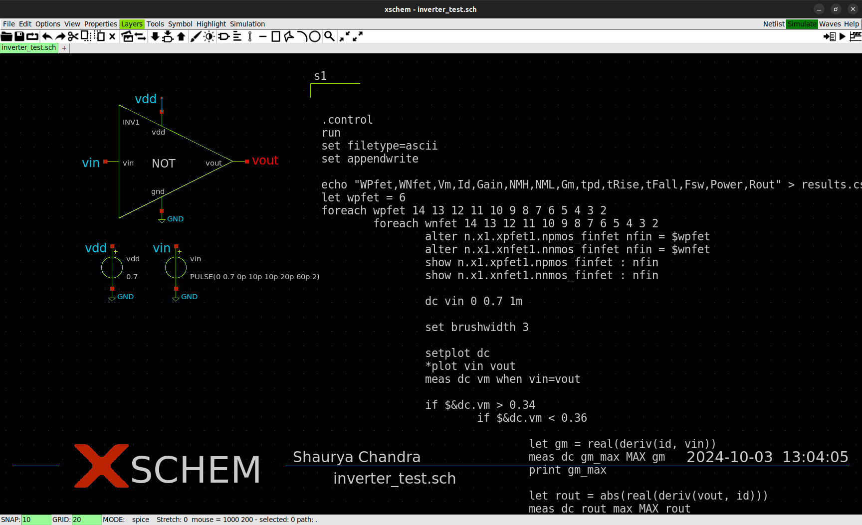
This Xschem schematic defines a setup for simulating an inverter circuit using FinFETs with varying transistor fin sizes. It includes sources for power and input, ground connections, and measurements for important metrics like delay, gain, noise margins, power consumption, and switching frequency. Here's a breakdown:
Testbench Components
-
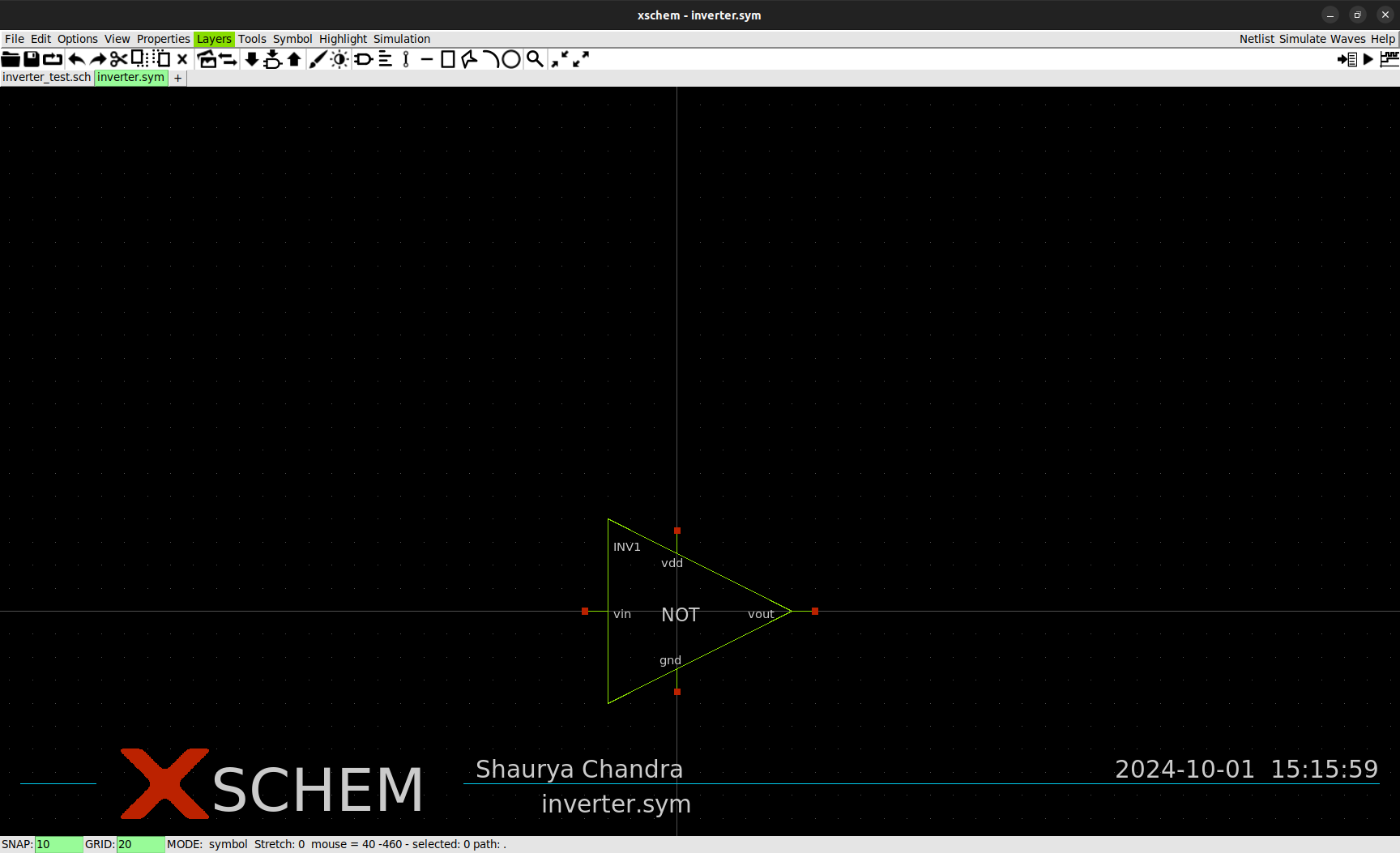
Inverter Design: The inverter (
inverter.sym) is placed in the circuit with connections to VDD, VIN, and VOUT. -
Voltage Sources:
- VDD is set to 0.7V.
- VIN is a pulse signal defined as
"PULSE(0 0.7 0p 10p 10p 20p 60p 2)", representing a periodic input for the inverter.
-
Ground Connections: Three GND components connect to different parts of the circuit.
-
Pins: The schematic has labeled pins (e.g., VDD, VIN, VOUT) for signal clarity.
-
Script Component (
code_shown.sym): This section defines a control script in.controlblocks that automates simulations, sweeping through different fin sizes for the nFET and pFET transistors (from 2 to 14 fins).- The simulation is carried out using NGSpice to observe the inverter's voltage transfer characteristics (VTC). The Vin is swept from 0 to VDD, and Vout is measured at different points to capture the inverter's response.
- It performs a DC analysis to find the voltage at which VIN equals VOUT (Vm), as well as measures metrics like gain, output resistance, and noise margins (NMH and NML).
- It also conducts transient analysis to measure timing metrics like rise and fall times, propagation delay, and switching frequency.
- Power consumption is calculated based on current through the VDD source.
The results are saved to a CSV file (results.csv) with fields for WpFET, WnFET, Vm, Id, gain, NMH, NML, Gm, propagation delay (tpd), rise time (tRise), fall time (tFall), switching frequency (Fsw), power, and output resistance (Rout).
Spice Deck Components
This section explains how the .control block inside the schematic automates the simulation process and captures the key performance metrics of the FinFET-based inverter across different transistor fin configurations.
1. Simulation Setup
This block initializes the simulation environment and sets the file type and output formats.
run: Starts the simulation process.set filetype=ascii: Specifies that results will be written in ASCII format.set appendwrite: Ensures that data is appended to the CSV file without overwriting it.
2. Result File Setup
echo \\"WPfet,WNfet,Vm,Id,Gain,NMH,NML,Gm,tpd,tRise,tFall,Fsw,Power,Rout\\" > results.csv: Creates a header row inresults.csvto store key metrics for each simulation iteration.
3. Transistor Fin Sweep
The nested loops adjust the number of fins for the nFET and pFET transistors, allowing performance analysis over a range of fin configurations.
foreach wpfet 14 13 12 ... 2: Loops through the values ofwpfet(fin size for pFET) from 14 to 2.foreach wnfet 14 13 12 ... 2: Loops through the values ofwnfet(fin size for nFET) from 14 to 2.alter n.x1.xpfet1.npmos_finfet nfin = $wpfet: Modifies the number of fins for the pFET in the inverter.alter n.x1.xnfet1.nnmos_finfet nfin = $wnfet: Modifies the number of fins for the nFET in the inverter.show n.x1.xpfet1.npmos_finfet : nfinandshow n.x1.xnfet1.nnmos_finfet : nfin: Displays the fin count for each transistor for verification.
4. DC Analysis
dc vin 0 0.7 1m: Performs a DC sweep of the input voltage (vin) from 0 to 0.7V, with a step size of 1mV.meas dc vm when vin=vout: Captures the Threshold Voltage (Vm) wherevinequalsvout.
Conditions:
- The midpoint voltage (
vm) is checked to ensure it lies between 0.34V and 0.36V. Only if this condition is satisfied, the transient analysis and metric calculations are performed.
5. DC Characteristics
Upon satisfying the voltage conditions, the script calculates the following VTC:
-
Gain:
let gm = real(deriv(id, vin)): Computes the transconductance (gm), which is the derivative of current (id) with respect tovin.meas dc gm_max MAX gm: Records the maximum gain value during the sweep.
-
Output Resistance:
let rout = abs(real(deriv(vout, id))): Measures the output resistance.meas dc rout_max MAX rout: Captures the maximum output resistance.
-
Current:
let id = abs(vdd#branch): Measures the absolute current through the VDD source.meas dc id_max MAX id: Stores the maximum current value.
-
Noise Margins:
meas dc vil find vin when gain_scaled=0.7 cross=1: Measures the low noise margin (NML) by finding the input voltage when the gain reaches 0.7 during the first crossing.meas dc vih find vin when gain_scaled=0.7 cross=last: Measures the high noise margin (NMH) during the last crossing.let vol = 0andlet voh = 0.7: Sets the logic high (voh) and logic low (vol) values to compute NMH and NML.
6. Transient Analysis
tran 0.02p 125p: Runs a transient analysis for 125 picoseconds with a time step of 0.02 picoseconds.
Simulation Output | PFET_nfin = 14, NFET_nfin = 13 and Vth = 0.349V
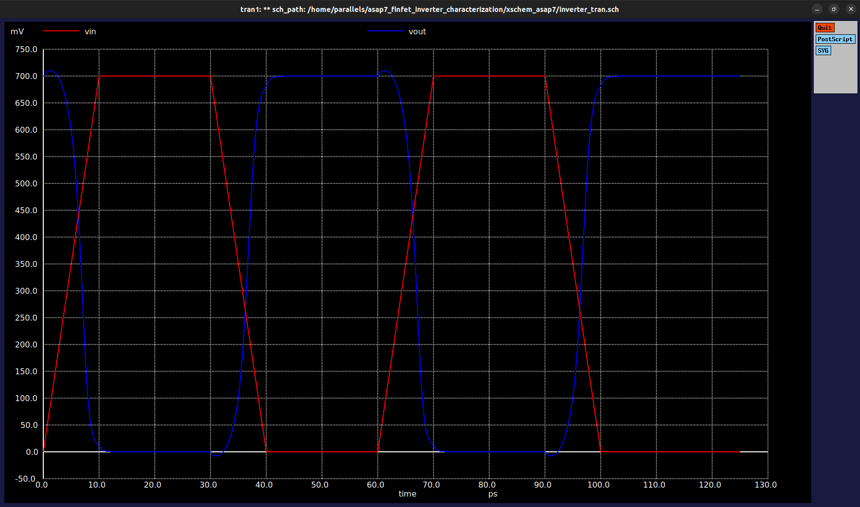
Timing metrics:
Note: The first transition may include noise or an unstable response due to initialization effects or transient settling. To avoid inaccuracies caused by initial conditions, it is common to ignore the first transition and use RISE=2 (or FALL=2), which measures the second complete transition when the circuit has settled into its periodic behavior.
-
Propagation Delay:
meas tran tin_rise50 when vin=0.35 RISE=2: Captures the input rise time at 50% of VIN.meas tran tout_fall50 when vout=0.35 FALL=2: Captures the output fall time at 50% of VOUT.meas tran tin_fall50 when vin=0.35 FALL=2: Measures the input fall time at 50% of VIN.meas tran tout_rise50 when vout=0.35 RISE=2: Measures the output rise time at 50% of VOUT.let tpd = (tpHL+tpLH)/2: Computes the average propagation delay (tpd) from high-to-low and low-to-high transitions.
-
Rise/Fall Time:
meas tran tout_rise90 when vout=0.63 RISE=2: Captures the 90% rise time of the output.meas tran tout_fall10 when vout=0.07 FALL=2: Captures the 10% fall time of the output.let tr = tout_rise90 - tout_rise10: Computes the total rise time.let tf = tout_fall10 - tout_fall90: Computes the total fall time.
-
Switching Frequency:
let fsw = 1/(tr+tf): Calculates the switching frequency (Fsw) based on rise and fall times.
-
Power Consumption:
meas tran id_integ integ id_tran from=60e-12 to=120e-12: Integrates the current over a period of time to estimate power.let power_int = id_integ*0.7: Multiplies the integrated current by the supply voltage (0.7V) to compute power.let power = abs(power_int/60): Calculates the average power consumption.
7. Result Output
echo \\"$wpfet,$wnfet,$&dc.vm,$&dc.id_max,$&dc.gain_max,$&dc.nmh,$&dc.nml,$&dc.gm_max,$&tran.tpd,$&tran.tr,$&tran.tf,$&tran.fsw,$&tran.power,$&dc.rout_max\\" >> results.csv: Appends the calculated metrics for each co.osdiation of nFET and pFET fins to the CSV file.
8. End of Control Block
.endcsignals the end of the control block..save all: Saves all signals and simulation data..end: Marks the conclusion of the script.
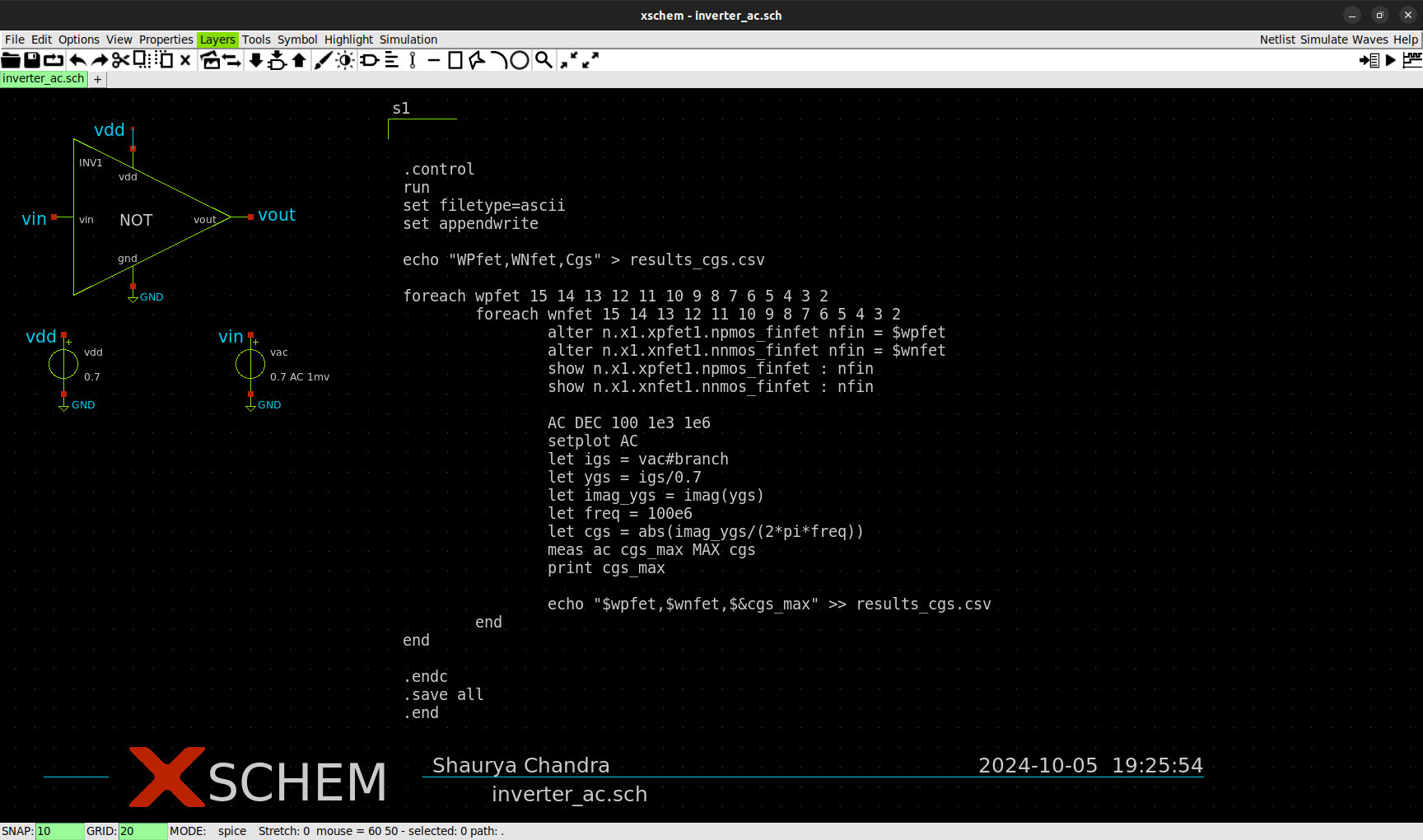
9. AC Analysis
The script runs an AC analysis across a range of fin configurations for both PFET and NFET transistors. The goal is to extract and record the maximum gate-source capacitance (Cgs) for each combination of fin counts.
The script performs the following steps:
- Fin Count Modification: The number of fins (
nfin) for both the PFET and NFET transistors are varied in nested loops. - AC Simulation: For each configuration, an AC analysis is run with 100 points per decade between 1 kHz and 1 MHz.
- Capacitance Calculation: Gate-source capacitance (
Cgs) is calculated based on the imaginary component of the admittance (ygs). - Data Logging: The maximum
Cgsvalue for each fin combination is appended to a CSV file (results_cgs.csv).
AC Simulation Spice Deck
.control
run
set filetype=ascii
set appendwrite
echo \"WPfet,WNfet,Cgs\" > results_cgs.csv

foreach wpfet 15 14 13 ... 2
  foreach wnfet 15 14 13 ... 2
    alter n.x1.xpfet1.npmos_finfet nfin = $wpfet
    alter n.x1.xnfet1.nnmos_finfet nfin = $wnfet
    AC DEC 100 1e3 1e6
    let igs = vac#branch
    let cgs = abs(imag(igs/0.7)/(2*pi*100e6))
    meas ac cgs_max MAX cgs
    echo \"$wpfet,$wnfet,$&cgs_max\" >> results_cgs.csv
  end
end
.endc
.save all
.end
4. Simulation Results
The Inverter_Pre_Layout_Sim_Results CSV file in the sim_results folder contains the key simulation parameters of a 7nm FinFET Inverter using the ASAP7 Process Design Kit (PDK), based on the BSIM4 CMG FinFET Model. The parameters captured during the inverter characterization include device dimensions, voltage metrics, timing, and power details.
- WPfet: Width of the PFET (in number of fins).
- WNfet: Width of the NFET (in number of fins).
- Vm: Inverter switching threshold voltage (V).
- Id: Drain current (A).
- Gain: Voltage gain of the inverter.
- NMH: Noise Margin High (V).
- NML: Noise Margin Low (V).
- Gm: Transconductance (S).
- tpd: Propagation delay (s).
- tRise: Rise time (s).
- tFall: Fall time (s).
- Fsw: Switching frequency (Hz).
- Power: Power consumption (W).
- Rout: Output resistance (Ω).
- Cgs: Input Gate Capacitance (F) ( 💡 doesnt inlcude overlap capacitance CGSO of PDK)
| WPfet | WNfet | Vm | Id | Gain | NMH | NML | Gm | tpd | tRise | tFall | Fsw | Power | Rout | Cgs |
|---|---|---|---|---|---|---|---|---|---|---|---|---|---|---|
| 15 | 14 | 0.349559 | 0.000233 | 6.42753 | 0.266 | 0.253 | 0.036222 | 1.64362e-12 | 3.89744e-12 | 3.65798e-12 | 1.32e+11 | 2.50619e-17 | 6.42753 | 1.28493e-20 |
| 15 | 13 | 0.354677 | 0.000224 | 6.42994 | 0.259 | 0.261 | 0.033675 | 1.67401e-12 | 3.90444e-12 | 3.72089e-12 | 1.31e+11 | 2.43233e-17 | 13.7203 | 1.2289e-20 |
| 14 | 12 | 0.355439 | 0.000208 | 6.43084 | 0.258 | 0.262 | 0.031090 | 1.73524e-12 | 3.97301e-12 | 3.79567e-12 | 1.29e+11 | 2.29834e-17 | 13.5661 | 1.1395e-20 |
| 13 | 13 | 0.344786 | 0.000210 | 6.42844 | 0.273 | 0.246 | 0.033599 | 1.73090e-12 | 4.03552e-12 | 3.72295e-12 | 1.29e+11 | 2.30893e-17 | 15.8751 | 1.16219e-20 |
