S100Computers T35 FPGA Module Design
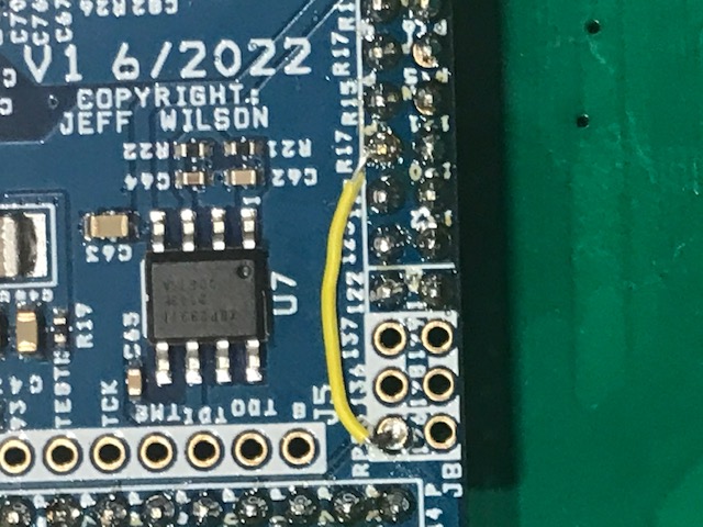
NOTE: See Important Wire Mod needed for Version 1b details at the end of page!
Table of Contents:
- Project Overview
- Toolchain
- Project Organization
- JTAG Programming Adapters
- Installing the FTDI Zadig USB Drivers
- Quick Start
- Design Files
- Important Wire Mod needed for Version 1b
- Jumper Assignments
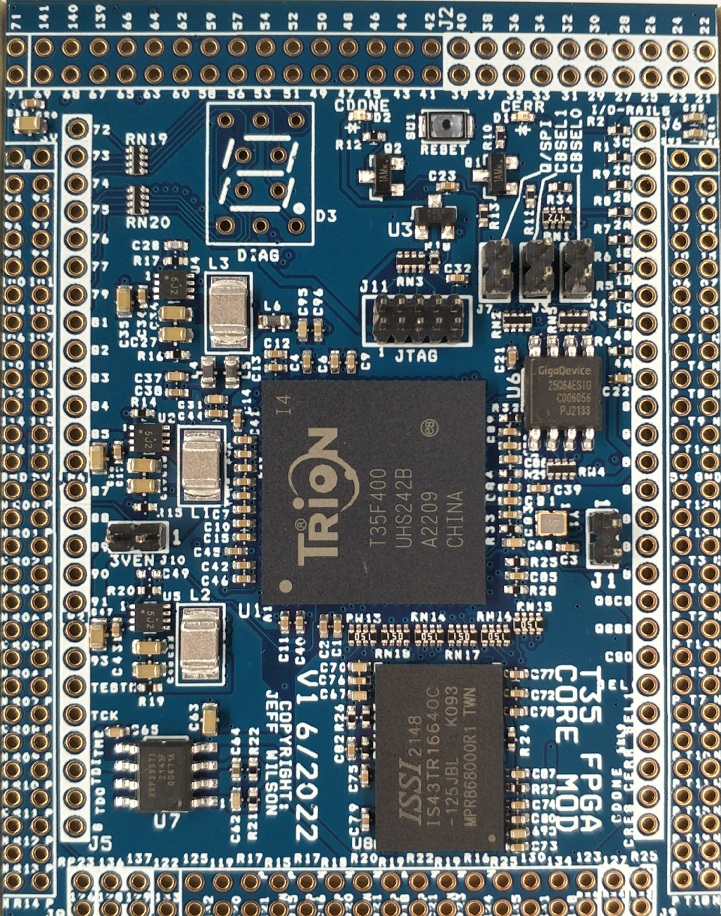
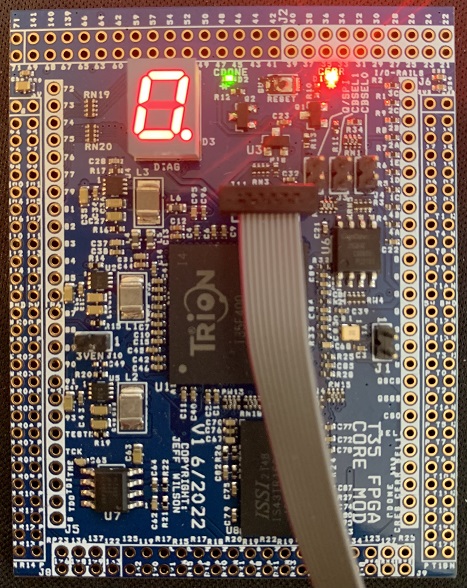
This is a custom T35 FPGA project module for S100Computers. This module was designed to augment the EP4CE10 based FPGA originally in use on the various FPGA S-100 Boards in the S100Computers inventory.
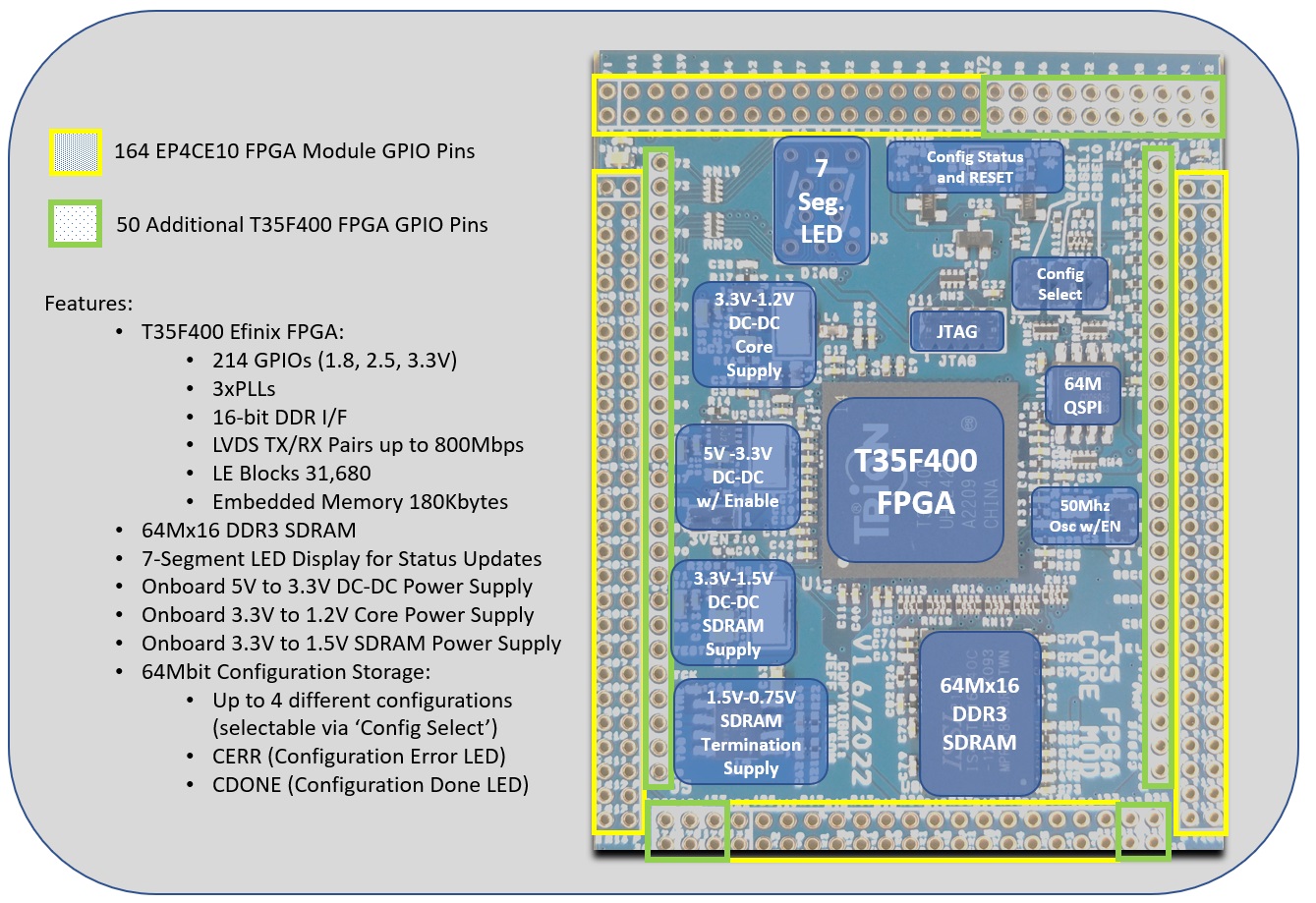
The module pictured below is in the same basic footprint as the original, but with added pins (shown in white-filled rectanges surroundng the new pins).
Added features in comparison to the original EP4CE10 module include:
- 50 Additional GPIO Pins for a total of 214 I/Os (Module is shipped with pins unmounted for added flexibility)
- 3x the Logic Elements (31,680 vs 10,320)
- 3.5x the Embedded FPGA RAM (180K vs 51K)
- Adds in LVDS Capability (up to 800Mbps)
- Adds 128MByte DDR3 SDRAM
- Up to four configuration images (jumper selectable)
- Seven Segment LED Display for custom status or diagnostic output
The FPGA Tool-chain used for this project is the EfinityIDE from Efinix Inc.
The Efinity IDE Toolchain is currently available with the purchase of an approved Efinity Development Board (see Efinix website for more details).
Projects for this board are generally stored on the root of the host system hard drive in the \S100Projects\ directory (e.g. - C:\S100Projects). The user does not need to replicate this directory structure, but there may be some project specific links that will need to be adjusted to move a project to a different directory organization.
The T35 FPGA Module uses a mini 5x2 JTAG Header with 0.05" (1.27mm) pin spacing. Mating cables and a JTAG Adapter PCB are available from Olimex that can be adapted for use in programming the T35 FPGA Module. The parts needed to implement this JTAG Programmer are available from Digikey and Mouser:
| Digikey Part No | Description | Manf | Manf Part No |
|---|---|---|---|
| 1188-1016-ND | JTAG Adapter | Olimex | ARM-JTAG-20-10 |
| 769-1106 | USB Adapter | FTDI | C232HM-DDHSL-0 |
| S2021EC-10-ND | Male to Male Header | Sullins | PRPC010DABN-RC |
| Mouser Part No | Description | Manf | Manf Part No |
|---|---|---|---|
| 909-ARM-JTAG-20-10 | JTAG Adapter | Olimex | ARM-JTAG-20-10 |
| 895-C232HM-DDHSL-0 | USB Adapter | FTDI | C232HM-DDHSL-0 |
| 649-77313-198-20LF | Male to Male Header | Amphenol | 77313-198-20LF |
The Olimex JTAG Adapter will need to be modified to fix a supply noise issue on the FTDI USB Adapter (where up to 700mV of noise is present on the FTDI 3.3V supply pin), and also to allow for the use of the Olimex JTAG Adapter with the T35 JTAG pinout.
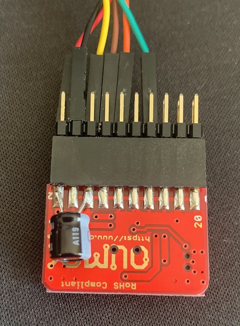
To fix the supply noise issue, a 100uF electrolytic cap must be added between pins 2 and 6 on the 20-pin female header:
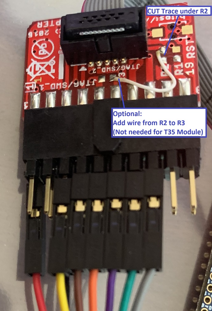
R2 on the Olimex JTAG Adapter (which is actually implemented as a trace/short) needs to be removed to avoid interfering with the Chip Select signal of the configuration flash on the T35 FPGA Module (pin 9 on the 10-pin Olimex header). See the Olimex JTAG Schematic.
To connect the USB Adapter to the Olimex JTAG, first plug in the 20-pin male to male header into the Olimex Female 20-pin header. Next plug the USB Adapter pin header cables into the following pins. When done you should have a color sequence of wires as shown above.
| JTAG Adapter Pin No | Color | Signal Name | T35 JTAG Pin No |
|---|---|---|---|
| Pin 2 | RED | +3.3V Supply | Pin 1 |
| Pin 5 | YELLOW | JTAG TDI | Pin 8 |
| Pin 6 | BLACK | GROUND | Pins 3 and 5 |
| Pin 7 | BROWN | JTAG TMS | Pin 2 |
| Pin 9 | ORANGE | JTAG TCK | Pin 4 |
| Pin 11 (Optional) | PURPLE | QSPI_CSN | Pin 9 |
| Pin 13 | GREEN | JTAG TDO | Pin 6 |
| Pin 15 | GREY | CRESET | Pin 10 |
(from Efinix AN006) The following instructions explain how to install a USB driver for Linux operating systems.
- Disconnect your board from your computer.
- In a terminal, use these commands:
    > sudo <installation directory>/bin/install_usb_driver.sh
    > sudo udevadm control --reload-rules
Note: If your USB JTAG Adapter was connected to your computer before you executed these commands, you need to disconnect and re-connect it.
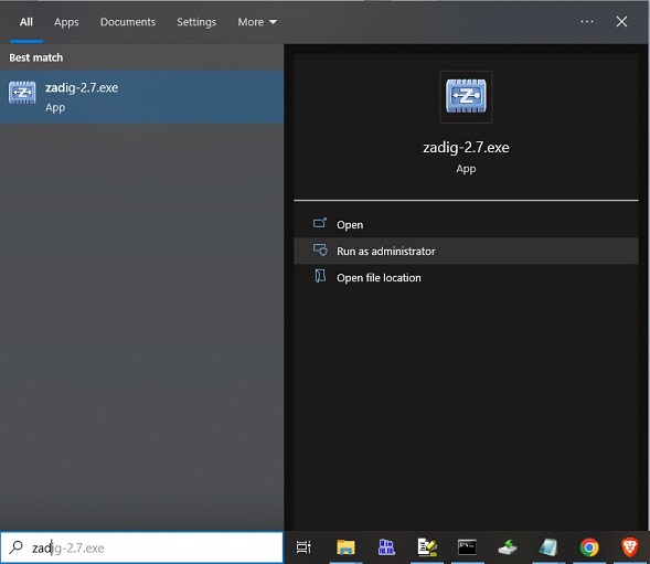
- Download Zadig from zadig.akeo.ie
- Copy the Zadig application from the 'Downloads' to a working directory.
- Right click the Zadig application and select "Run as Administrator".
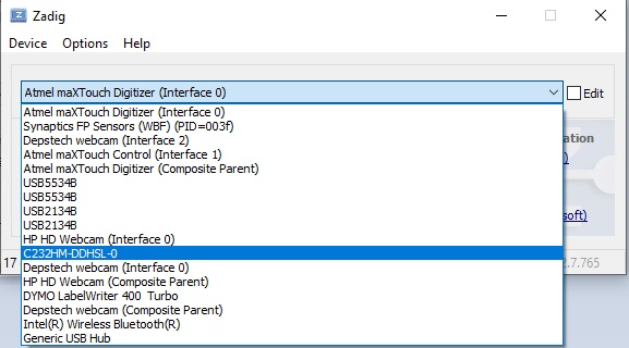
NOTE:Zadig can have problems identifying the C232HM-DDHSL-0 when other FTDI based USB devices are plugged in. Efinix recommends unplugging other FTDI devices while configuring the C232HM-DDHSL-0, after which you should be able to plug the other devices back in.
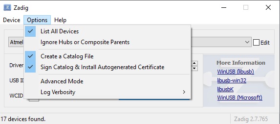
- Choose Options->List All Devices and turn off Options->Ignore Hubs or Composite Parents.
- Select C232HM-DDHSL-0 from the drop down list.
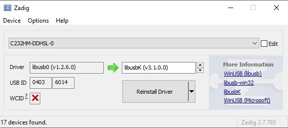
- Select libusbK from the drop down list.
- Click Reinstall Driver or Replace Driver.
Proceed to the Quick Start section below to verify correct operation of the JTAG Programmer.
(After toolset and driver install).
-
Create a new directory called T35seg7 under the C:/S100Projects/ directory (e.g. - C:/S100Projects/T35seg7/ ).
-
Download (Clone) the T35seg7 Test Project to the C:/S100Projects/T35seg7/ directory. This is a good initial project to use on existing S100Computers S-100 FPGA Boards as it does not drive any of the legacy WaveShare GPIOs; it only drives the GPIOs associated with the seven segment display (GPIOL_72 to GPIOL_81). This avoids any signal conflicts with exisiting designs. The purpose of this FPGA project is to count and display the numbers from 0 to 'F' (hexadecimal) on the seven segment display on one second boundaries.
-
Start the Efinity toolchain and load the C:/S100Projects/T35seg7.xml project.
-
Compile the T35seg7 project by clicking on the
 icon. (Wait for completion)
 -
Prepare for SPI FLash Programming by downloading and copying the jtag_spi_flash_loader.bit file into the /outflow/ directory. Doing this will allow the Efinity Programmer to find the JTAG Bridge bitstream file automatically when performing SPI Programming.
-
Connect the JTAG Adapter to the T35 JTAG port and plug the cable into a USB port. (NOTE: No other connections are necessary as the T35 FPGA Module can derive its power from either the module interface pins or the JTAG Cable). Be careful to align the red stripe of the JTAG cable to the left and make sure that the JTAG pins are properly aligned (it is possible to plug this connector in being one row off). When done the JTAG cable should hang straight down to the Olimex JTAG Adapter without looping (if looped, you may have the cable ends reversed).
There are two types of programming that can be done with the T35 FPGA Module:
- JTAG Programming (this targets the FPGA configuration RAM directly, but does not save it in Flash).
- SPI Flash Programming (this targets the SPI Configuration Flash for confiuration auto-load on power on).
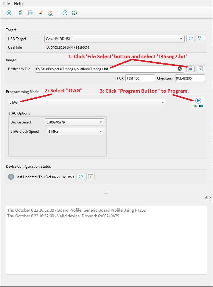
- Click the "File Select" Button
 and select the T35seg7.bit configuration bitstream from the open file dialog box.
 - Under "Programming Mode" select "JTAG" from the drop-down menu.
- Click the "Program Button"
 to program the T35 via JTAG.
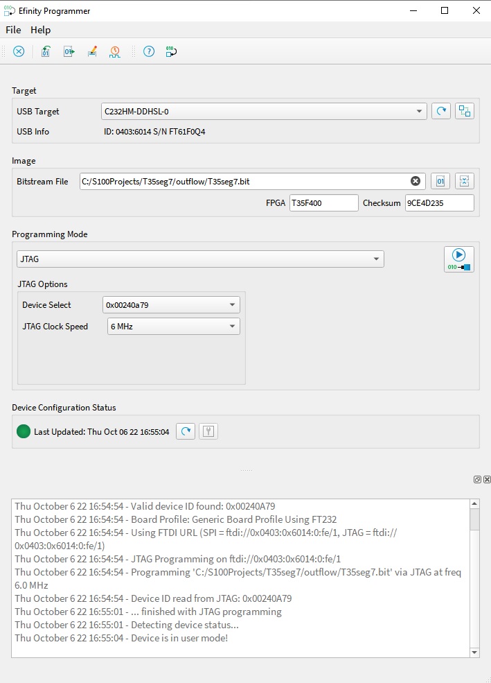
Once programmed, you should see the T35 transition into User mode:
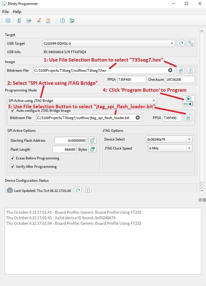
- Click the "File Select" Button
 and select the T35seg7.hex configuration bitstream from the open file dialog box.
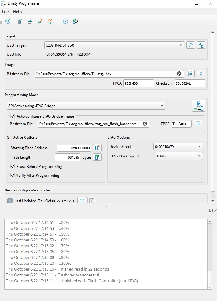
 - Under "Programming Mode" select "SPI Active using JTAG Bridge" from the drop-down menu.
- Use the "File Select" button in the "Auto configure JTAG Bridge Image" to select the downloaded jtag_spi_flash_loader.bit in the outflow directory. (Efinity should have already recognized the bridge image in the outflow directory, but if it doesn't, make sure to select it before proceeding).
- Click the "Program Button"
 to program the T35 via JTAG.
The programmer will now erase and then program the T35seg7 bitstream image into the flash.
After programming, you should see a "Flash verify Successful!" message when done:
NOTE: Since the jtag_spi_flash_loader.bit bitstream is still loaded into the T35's configuration RAM after programming, you will need to press the reset button on the module to have the T35 load the new configuration from the flash.
T35 FPGA Module Pin Assignments (with special thanks to Terry Fox!)
| Jumper Ref Des | Function | Default Setting |
|---|---|---|
| J1 - OSC DIS | On Board Oscillator Disable | Open (Osc Enabled) |
| J3 - CBSEL1 | Config Binary Select: | Open (Image 0) |
| J4 - CBSEL0 | [00, 01, 10, 11] | Open (Image 0) |
| J7 - QSPI/SPI | QSPI vs SPI I/F Config | Open (QSPI) |
| J10 - 5V-3V EN | 5V to 3V SMPS Enable | Open (5V-3V Disabled) |
| J11 - JTAG | JTAG Connector for Programming | N/A |
NOTE: J7 is only used for initial manufacturing board qualification and testing of new Configuration Flash Devices. Leave OPEN for normal module use.
- J1 - Allows for disabling the on-board oscillator to allow for the use of an external oscillator on J6 pin 23.
- J3/J4 - Allows for programming and selection (at boot) of multiple configuration binary images.
- J7 - Used for qualifciation of new configuration flashes (not normally used by users - leave open)
- J10 - Allows for enabling the on-board 5V to 3.3V DC-DC Converter (SMPS) for hosts that DO NOT SUPPLY 3.3V to the T35 Module.
- J11 - 10 pin 0.050" Mini JTAG Header for programming and configuration.
There is an important single wire modification needed for complete compatibility with the WaveShare pinout due to a missing PCB net on DC1D pin 148 (please see schematic above for details).
