These are tutorials translated from the mist project to work with MiSTer.
This part of the tutorial was presented in issue 26 '15 of the c't magazine.
Each lesson presented here explains a single aspect of the MiST board. The lessons are not VHDL or Verilog tutorials. Instead the lessons include all files required to build demo setups for the MiST board. They come with compiled and synthesised binaries so you can test run them before getting into the details.
Each lesson focuses on one aspect like the VGA output, then SDRAM, the SD card etc etc. Most lessons use a VHDL Z80 CPU and implement a small but fairly complete system on a chip (SoC) which can be used to experiment with the lessons. But it can also be used as a basis for bigger systems.
The intended audience of this are people who already have some basic VHDL or Verilog knowledge and know how to use a tool like Quartus and who want to learn how to use the various peripherals on the MiST board.
Unless otherwise stated all code included comes without restrictions and you can re-use it in any way be it for closed source or open source projects. Most included third party code (T80, YM2149, PS2) comes under GPL or simimlar license and may e.g. not be used closed source projects or the like. Please have a closer look at the files you intend to re-use for your project
Lesson 1: A VGA controller
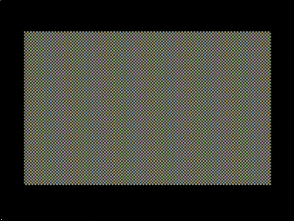
A 160x100 pixel VGA controller based on the 640x400@70Hz VGA mode. A simple b/w checkerboard is being displayed. The Video clock of 25.175 MHz is generated from the 27 MHz system clock using a PLL.
The VGA controller mainly consists of the two counters, one to count the pixels per line (h_cnt) and one counting lines (v_cnt). Both counters are used to generate the horizontal and vertical sync signals and to determine the time where pixels are to be displayed. The horizontal counter is directly updated by the pixel clock. The vertical counter is updated once per line only.
The VGA controller has six output bits per color. On the MiST board these are fed into a resistor ladder (r2r) which is used as a digital analog converter to generate the analog video signals. Six bits are sufficient for 2^6=64 shades per color resulting in a total of 262144 colors in total. Using PWM techniques more colors are possible. E.g. the Amiga AGA core does that. This demo however just displays a black'n white checkerboard.
Links:
Lesson 2: Video memory and embedded ROM
The VGA controller is now being equipped with 16000 bytes of embedded FPGA RAM as video memory (VMEM/VRAM). The resulting video controller can display 256 colors in RGB 332 format (3 bits red, 3 bits green, 2 bits blue). A demo image is placed into an embedded ROM and copied into screen memory at start up.
The graphics needs to be in 160x100 pixels in RGB332 format. The img2hex.sh shell script uses the Linux tool "avconv" (on older distros it may be named "ffmpeg") to generate a matching raw image from a 160x100 pixel PNG image. The resulting raw image is exactly 16000 bytes in size. img2hex.sh then calls the srec_cat to convert this into intel hex format.
The ROM has been generated using Quartus' Megafunction wizard. It allows to specify a intel hex file as the data source for the ROM.
Lesson 3: Z80 CPU and RAM
The T80 Z80 CPU core is being added. 4 kilobytes of RAM are added for the CPU as well as 4 kilobytes of ROM. ROM and VRAM share the same memory region as ROM is read only and (our) VRAM is write only. On most systems video memory can be read and written which is quite useful when altering video contents. In our SoC we implement the video memory write only which is not the usual way to do it. But a platform like an FPGA allows us to do this and if it turns out to be a bad idea we can easily change this. But being able to map VRAM and ROM to the same address space makes efficient use of the 64k address space the Z80 CPU offers.
The CPU is clocked at 4 Mhz which is additionally to the VGA clock generated by the existing PLL.
The ROM contents are compiled from a C source using the SDCC compiler (http://sdcc.sourceforge.net). SDCC generates a intel hex file which is directly included into the ROM by Quartus' Megafunction wizard like the image data in lesson 2.
All memory is decoded only partially which means that the 4k ROM at address 0x0000 is mirrored 7 times in the lower 32k memory area (A15=0). The ROM shows up at addresses 0x0000-0x0fff, 0x1000-0x1fff, 0x2000-0x2fff, 0x3000-0x3fff, 0x4000-0x4fff, 0x5000-0x5fff, 0x6000-0x6fff and 0x7000-0x7fff. The 16000 bytes video of video memory is mapped twice and can be written at address 0x0000-0x3ef7 and 0x4000-0x7e7f. Finally the 4K RAM is mapped to the upper half of the address space (A15=1) and can be read and written at 0x8000-0x8fff, 0x9000-0x9fff, 0xa000-0xafff, 0xb000-0xbfff, 0xc000-0xcfff, 0xd000-0xdfff, 0xe000-0xefff and 0xf000-0xffff. The SDCC compiler by default uses 0xffff for the stack going downwards and it used the memory region from 0x8000 for global variables. The aforementioned mirroring allows to use the default SDCC memory layout with only 4k RAM. We can do this as long as we don't need the address space for other purposes.
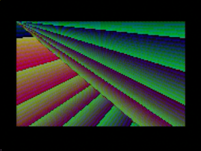
The test program is a simple graphics demo. It doesn't use any global variables but uses the stack for local variables. Thus the running demo shows that ROM as well as RAM are working as well as the video memory, of course.
Links:
Lesson 4: SDRAM
So far we've been using FPGA internal embedded RAM. This is very easy to implement and use and incredibly fast. Unfortunately there's only a little more than 70 Kilobytes of embedded memory available inside the MiST's FPGA. Therefore the MiST comes with additional 32MBytes SDR-SDRAM.
SDR-SDRAM is a more modern memory type than the DRAM that was used in the homecomputer age. But it's also significantly older than the latest DDR4/5-SDRAM memories todays computers use. The latest memory types can be very fast under certain conditions but are very complex to control. The usage of SDR-SDRAM was a useful tradeoff between speed and ease of use. Furthermore modern RAMs don't match the retro requirements very good.
The MiST comes with a 133MHz 16 bit wide SDR-SDRAM. This means that the RAM can be clocked at up to 133 Mhz and that it transfers 16 bits (two bytes) at once. A SDR-SDRAM uses a synchronous protocol to access its contents unlike DRAM which was asynchronous. In the first access stage (RAS cycle) a part of the desired address information is sent into the SDRAM. After a certain pause the second half of the address information (CAS cycle) is sent to the SDRAM and finally after another pause the data itself can be read or written. The lengths of these pauses depend on certain SDRAM parameters and on the clock that's actually being used to access the SDRAM.
On the MiST a typical single SDRAM transfer requires 8 clock cycles. Thus the SDRAM is typically clocked at 8 times the CPU clock so the SDRAM can perform a full access cycle during one CPU cycle. Since the CPU is clocked at 4 Mhz in our SoC the SDRAM is clocked at 32Mhz. The 32Mhz are again generated by our PLL and the 4Mhz are now derived from the 32Mhz by dividing it by 8.
There is a counter "q" inside the SDRAM controller sdram.v which
permanently counts from 0 to 7. This counter synchronizes itself to the
CPU clock to make sure the counter always starts with 0 at the begin
of a CPU cycle. When running at 32Mhz and with one full memory
transfer every 8 cycles the resulting total access time is 250ns. This
was a typical RAM access rate in the age of home computers. The SDRAM
supports a clock of 133Mhz and thus access times of ~60ns are
possible. Special burst access modes of the SDRAM can be used to read
more than 16 bits in one access cycle. But these must be consecutive
memory contents and require a CPU to have caches to increase the
system performance. Retro CPUs usually don't have that. The limit for
single random accesses is ~60ns (this is actually still the same with
modern DDR RAM).
The SDRAM has a 16 bit data bus but our SoC is a 8 bit system. We thus simply ignore one half of the data bus. As a result only 16 of the 32 MBytes can be addressed. This is still much more than the Z80 can easily handle. The Z80 has a 16 bit address space giving a total of 64 kBytes directly accessible memory. The SoC is currently using the upper half of this for RAM. Thus only 32 kBytes of the SDRAM is actually being used. It would be possible to implement banking or the like to give the Z80 access to more memory. But this requires special support in the software which we'd like to avoid.
SDRAMs need to be initialized before they are fully operational. The
sdram.v contains a simple logic to do this once the PLL reports that
it's generating stable clocks via its locked signal. The CPU is being
kept in reset a little longer to make sure the SDRAM is ready once the
CPU starts running.
The SDRAM timing is quite critical. One result of this is that a second 32Mhz clock is generated by the PLL with a small offset (phase shift) of -2.5ns. This clock is fed into the SDRAM. This makes sure that the FPGA and the SDRAM aren't changing signals at exactly the same time. Instead one of them changes signals on one clock and the other component sees stable signals when it's own slightly shifted clock changes.
Further stability is added by the soc.sdc constraints file. This tells Quartus about timing critical signals. Quartus will then make sure these signals need to be connected in a way that they have a minimum delay.


