Table of Contents
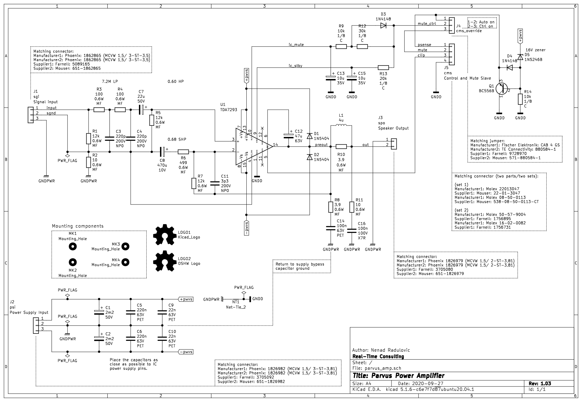
This document shall describe rationales used to design and build audio power amplifier using TDA7293 integrated circuit.
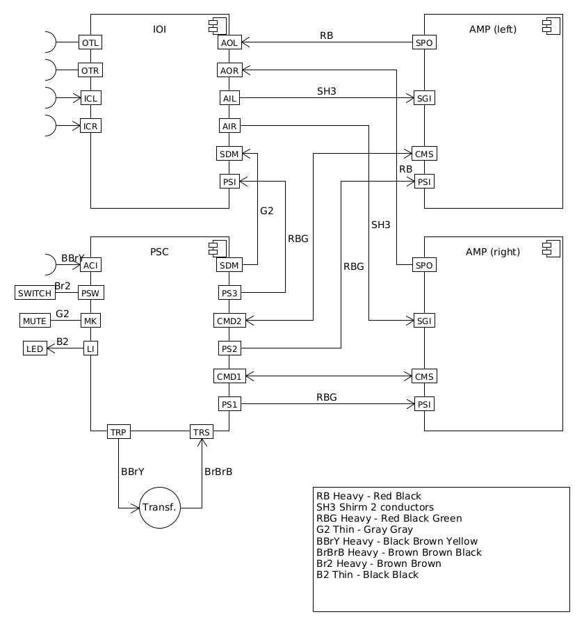
The amplifier architecture consists of the following sections:
- The amplifier consists of the following section:
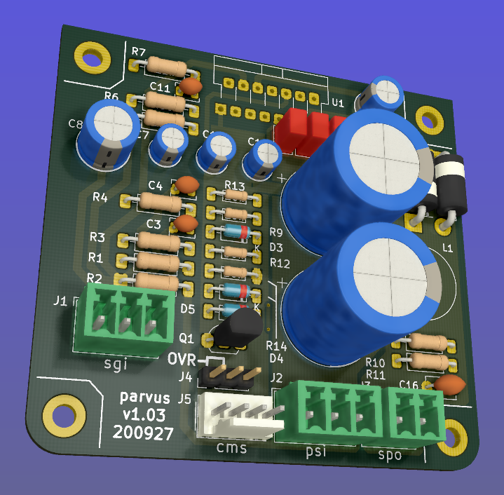
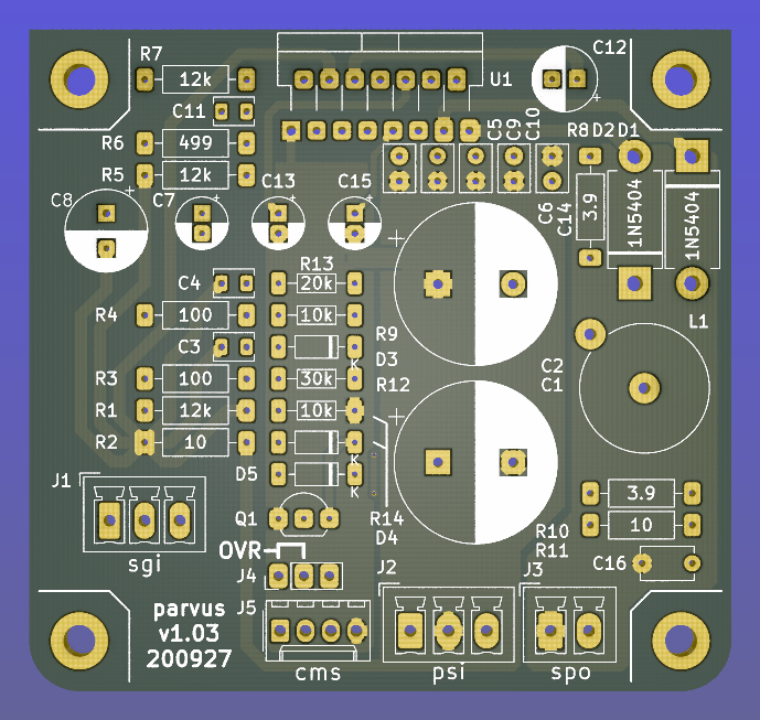
- Amplifier (AMP) board (left and right channels)
- Input/output filtering and Interface (IOI) board
- Power supply and control (PSC) board
Each of these sections are implemented as a separate board.
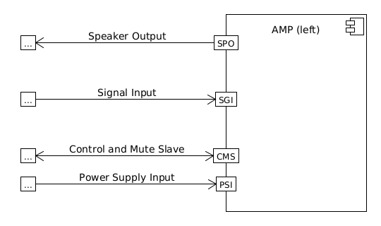
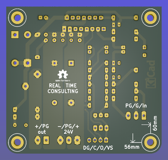
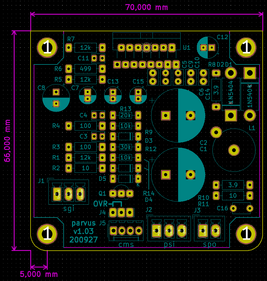
The board features the following conntectors:
- Power Supply Input - PSI: Vcc, GND, Vee
- Speaker Output - SPO: Out, GND
- Signal Input - SGI: In, SGND
- Control and Mute Slave - CMS: Power sense, Mute, Clip, GND
For input filter we choose the frequency between 300kHz and 400kHz:
    +---+ Rlp1    +---+ Rlp2
0---+   +----+----+   +---+---o Toward Amplifier IC block
    +---+    |    +---+   |
           ----- Clp1   ----- Clp2
           -----        -----
             |            |
            === Ground   === Ground
Using the 2nd order CR low-pass filter calculator at URL: http://sim.okawa-denshi.jp/en/CRCRtool.php we arrive at:
Rlp1 = 100 Ohm, Rlp2 = 100 Ohm
Clp1 = 220pF, Clp2 = 2.2nF
fp1 = 352kHz
fp2 = 14MHz
For more details please refer to: http://www.johnhearfield.com/RC/RC4.htm
A ground loop breaker resistor is located between SGND and GNDPWR grounds. The value of this resistor should be around 10 ohms.
Using inverted topology since we want to reduce common mode distortion in the input stage. But in case of TDA7293 IC it is not easy to use inverted topology since the mute circuit is implemented on positive OPAMP input.
The equivalent gain circuit resistance needs to stay below 600ohms. This is so because all noise measurements in data-sheet were done with 600ohms or 0ohms.
- Using low feedback gain is preferred for several reasons:
- there is more loop gain available to reduce the distortion
- reduced outout noues
- lower offset at output
Nominal gain of an non-inverting amplifier is:
G=Rf/Rg+1
Since we have a voltage divider with same resistors in the front of the amplifier the total gain becomes:
G=Rf/Rg
The minimum gain specified in the TDA7293 datasheet is 26dB or 20 times. Just to be on the safe side we choose 10% bigger value: 22
- Chosen values for E24 series:
- Rf = 12kOhm
- Rg = 510 Ohm
- Chosen values for E48 series:
- Rf = 11kOhm
- Rg = 499 Ohm
The TDA7293 data-sheet does not provide enough of relevant data in order to
model the IC in AC domain. Since we can't model it there are no optimizations
available for the negative feedback circuit. But we can safely assume that
there are high frequency poles present in the TDA7293 transfer function. For
this reason we will add a few pF to calculated lead compensation
capacitor below (see Cadd).
Equivalent feedback network with lead compensation circuit:
       o Vout
       |
       *------+
       |      |
      +-+ Rf  |
      | |   ----- Cf=Cl (+Csi, see Input pin capacitance compensation)
      | |   -----
      +-+     |
Vf     |      |
 o-----*------+
       |
      +-+ Rg
      | |
      | |
      +-+
       |
       o Input
Resistors Rf and Rg are part of feedback network. Capacitor Cf is the compensation capacitor. The transfer function of this network is given as:
Vf(s)=I(s)*Rg
Vout(s)=I(s)*(Rf||Cl + Rg)=I(s)*(Rf/(1+s*Rf*Cl)+Rg)
H(s)=Vf(s)/Vout(s)=(Rg/(Rf+Rg))*((1+s*Rf*Cl)/(1+s*Re*Cl))
Zero:
wz=1/(Rf*Cl)
Pole:
wp=1/(Re*Cl)
Where:
Re=Rf||Rg=Rf*Rg/(Rf+Rg)
Rough estimation is to put additional 1-3pF in parallel to Rf.
Cadd = 3pF
Input pins have the following parasitic capacitances associated:
- Cdiff
- Cm
- Cstray
The TDA7293 data-sheet does not specify any parameter regarding parasitic input capacitances. Voltage feedback OPAMPS usually have both differential and common-mode input impedances specified. In the absence of any information, it is safe to use the model given in the next figure:
               +----+ Zdiff
+input o---+---|    |---+---o -input
           |   +----+   |
           |            |
          +-+ Zcm1     +-+ Zcm2
          | |          | |
          | |          | |
          +-+          +-+
           |            |
          ===          ===
We can use a rough estimation of values based on experience on using other
audio FET OPAMPS, and typical values are around Cdiff=5pF, Cm=4pF
and Cstray=3pF. All three equivalent capacitors are tied in parallel,
so the total input capacitance becomes:
Cinput = Cdiff+Cm+Cstray=5pF+4pF+3pF=12pF
To mitigate this capacitance we can add capacitance Csi parallel to Rf resistor. To compensate for this the following equation is applied:
Rf*Cf=Rg*Cinput
Csi=Cinput*Rg/Rf=0.5pF
The final Cf value is:
Cf=Cl+Csi+Cadd=0+2+0.5=2.5pF
Any NP0 based capacitor around 3pF will be good for this purpose.
To protect the input from EMI we will use the following Zobel network:
  o Positive input or negative input
  |
  |
----- Czi
-----
  |
  |
 +-+  Rzi
 | |
 | |
 +-+
  |
 === Ground
For most input cables characteristic impedance falls in range between
50 and 100ohm impedance and we are using the 75ohm as the middle value. The
resistor Rzi is Rzi=75ohm and the capacitor Czi is Czi=220pF.
This network should be placed right at the input connector, not on the
main amplifier PCB.
Also, a 100n X7R capacitor shall be placed between SGND and chassis right at the input connector. This capacitor will shunt radio and other interfirence signal into the Chassis Ground potential.
Output network consists of upstream and downstream Zobel Network and of output
coil (Ld) with parallel, damping resistor (Rd). Upstream Zobel network
provides a low-inductance load for the output stage at very high frequencies
and allows high-frequency currents to circulate local to the output stage. The
downstream Zobel network provides a good resistive termination right at the
speaker terminals at high frequencies, helping to reduce RFI ingress and damp
resonances with, or reflections from, the speaker cables.
The output circuit is the following:
         Ld
         xxx
    +---x   x   x---+
    |        xxx    |
    |               |
    |   +-------+   |
o---+---|       |---+---o
Vout    +-------+   |   Vspeaker
    Rd              |
                  ----- Cz2 = 100nF
                  -----
                    |
                    |
                   +-+  Rz1 = 10 Ohm
                   | |
                   | |
                   +-+
                    |
                   ===
The output coil Ld provides high frequency isolation of output load from
output stage in TDA7293. The inductance value should be between 2uH up to 5uH.
Output shunt resistor should be between 2 and 5 Ohms. See
Douglas Self - Audio Power Amplifier Design Handbook, 3rd Ed., Output networks, chapter 7
for effect on power amplifier transfer function.
The power supply section is using single bank of 10mF capacitors.
We are using dual symmetrical supplies from since dual secondaries.
The main voltage supplies are supplied directly from reservoir capacitors. This supply powers the high current, high power output sections of TDA7293.
Before rectifier diodes a snubber RC circuit should be placed to decrease diode
switching impulse. Recommended values are Rsn = 1 Ohm, Csn = 470nF:
  o Vsupply
  |
  |
----- Csn = 470nF
-----
  |
  |
 +-+  Rsn = 1 Ohm
 | |
 | |
 +-+
  |
 === Ground
This snubber may be placed near the IC power supply lines, too.
- NOTE:
- On case chassis there should be a safety ground screw just near at the input 220V socket.
Power supply capacitors on amplifier boards:
- 30mm (10mF)
