Monome Norns Shield SMD Guide / FAQ
Two principles for SMD assembly:
Order of Operations : A sequence of actions with consideration of the past, present, and future.
Economy of Motion : Save time and energy = work faster and more accurately.
By utilizing Order of Operations , the most difficult to source components are placed last to prevent having to remove them.
By utilizing Economy of Motion and moving around the board in a specific manner, you can reduce confusion, placement errors, and loss of components.
Before we begin, essential basics:
Inventory – Carefully check the BOM and make sure that you have everything before you begin. The SMD portion can be completed in one session. Incomplete SMD projects often remain so.
Tools - Unleaded solder requires higher heat. The most common problem I see on Shield builds are cold solder joints. Turn up the heat and work quickly. The modern TS80 type irons are high quality and can do a lot of this work, but only if you use proper heat. Check the data sheet or packaging of your solder and set the temperature accordingly. Use flux during assembly and isopropyl alcohol (99%) to properly clean the board. You will need to clearly see what is happening, especially on the fine pitch components.
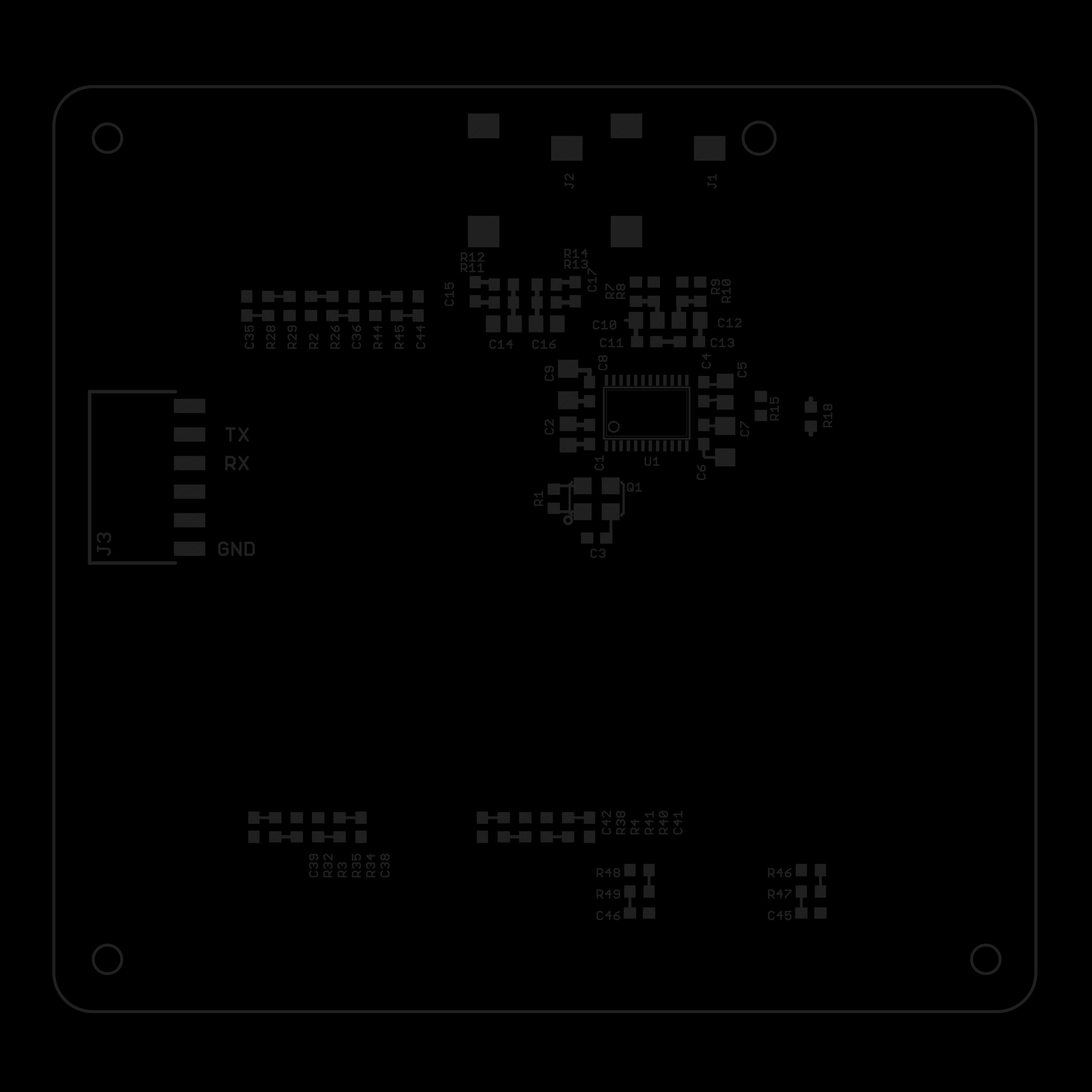
A bare Norns Shield PCB, do the SMD work before the through hole work.
(through hole guide is available here https://github.com/monome/norns-shield )
This guide uses the MFG part numbers from the Octopart BOM, placement order descending from highest quantity to lowest quantity.
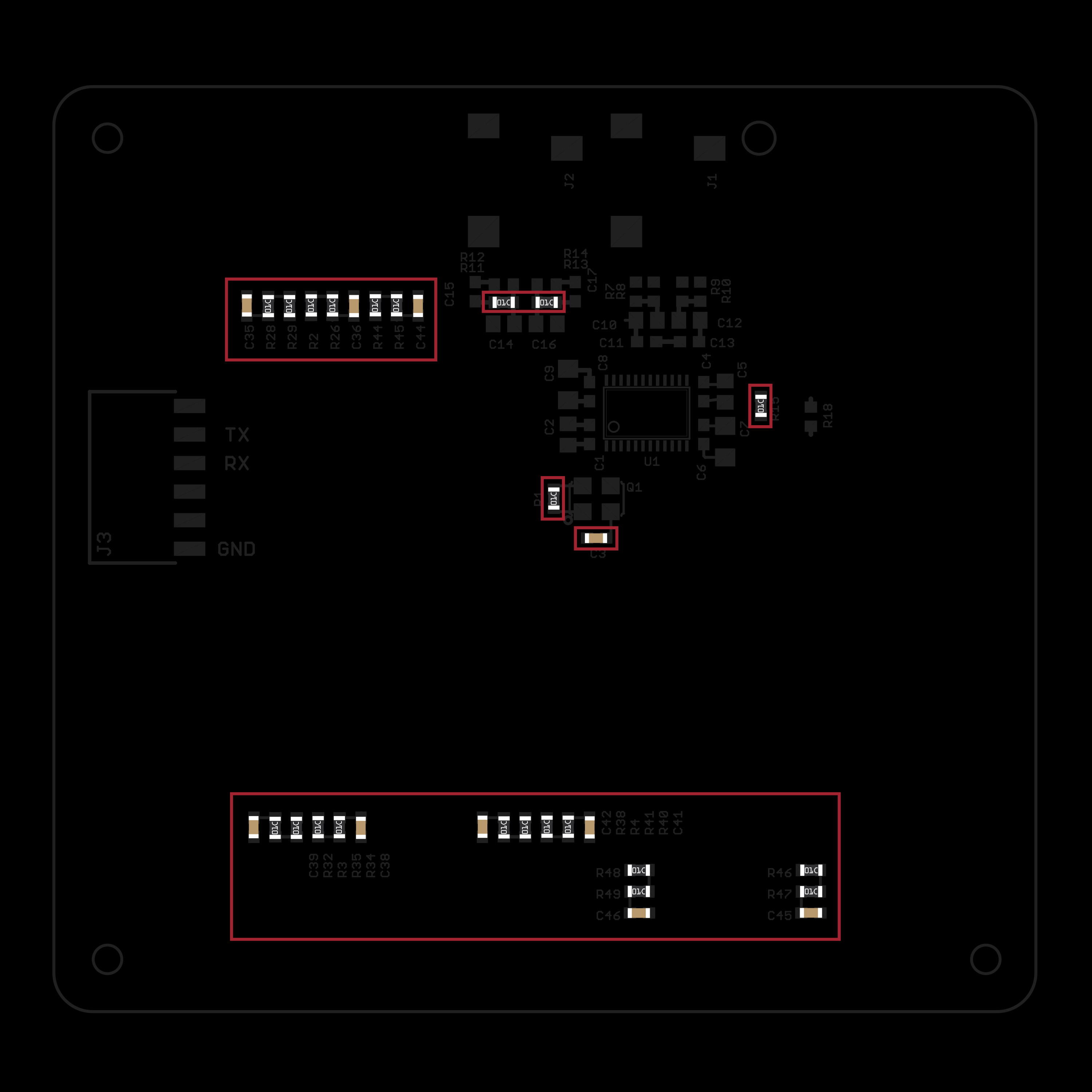
In the areas indicated in RED place:
10k Resistors (MFG P/N RC0603FR-0710KL, code O1C)
R1, R2, R3, R4, R11, R13, R15, R26, R28, R29, R32, R34, R35, R38, R40, R41, R44, R45, R46, R47, R48, R49
10000pf Capacitors (MFG P/N CC0603KRX7R9BB103, Light brown in color)
C3, C35, C36, C38, C39, C41, C42, C44, C45, C46
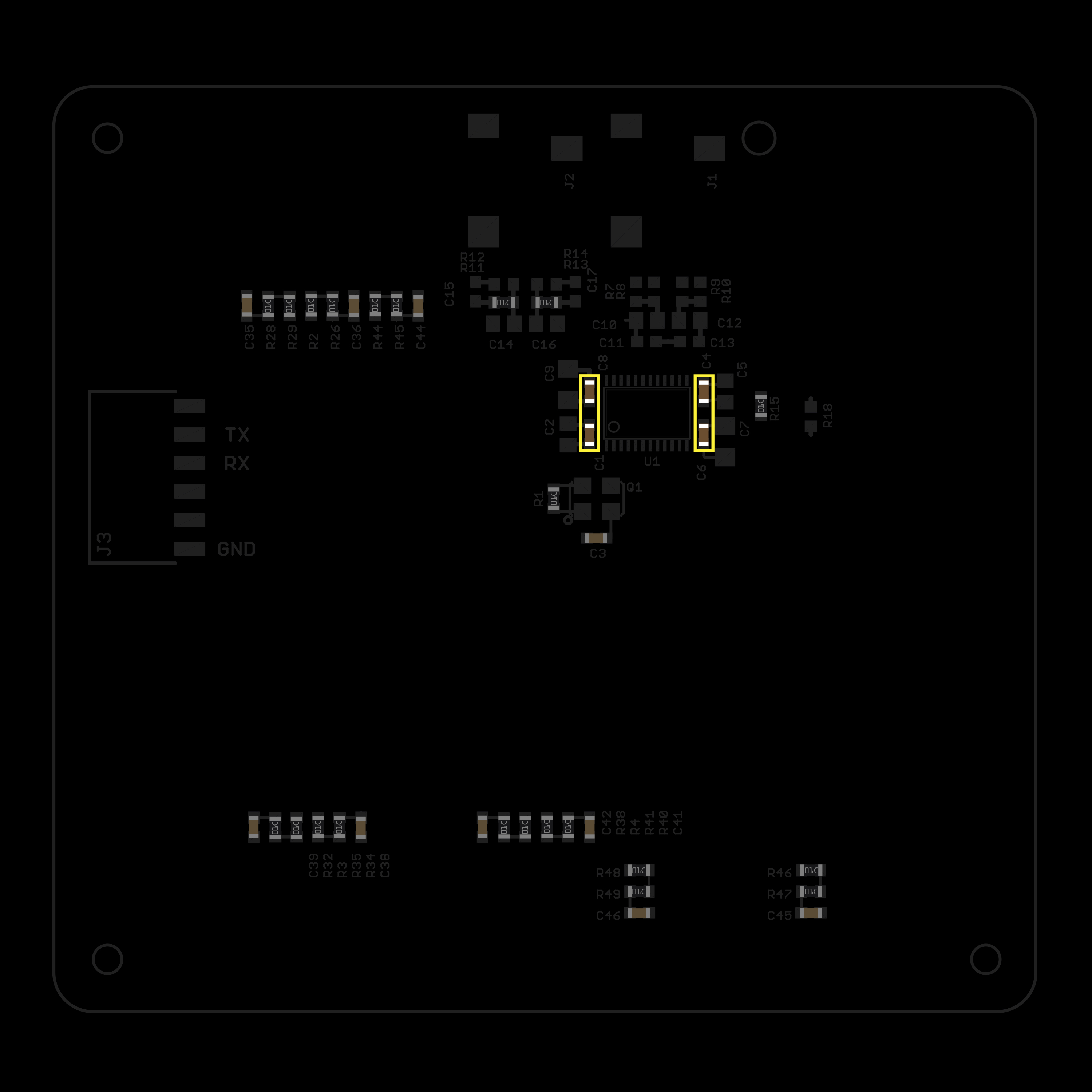
In the area indicated in YELLOW place:
0.1uF Capacitors (MFG P/N CC0603ZRY5V9BB104, brown in color)
C1, C4, C6, C8
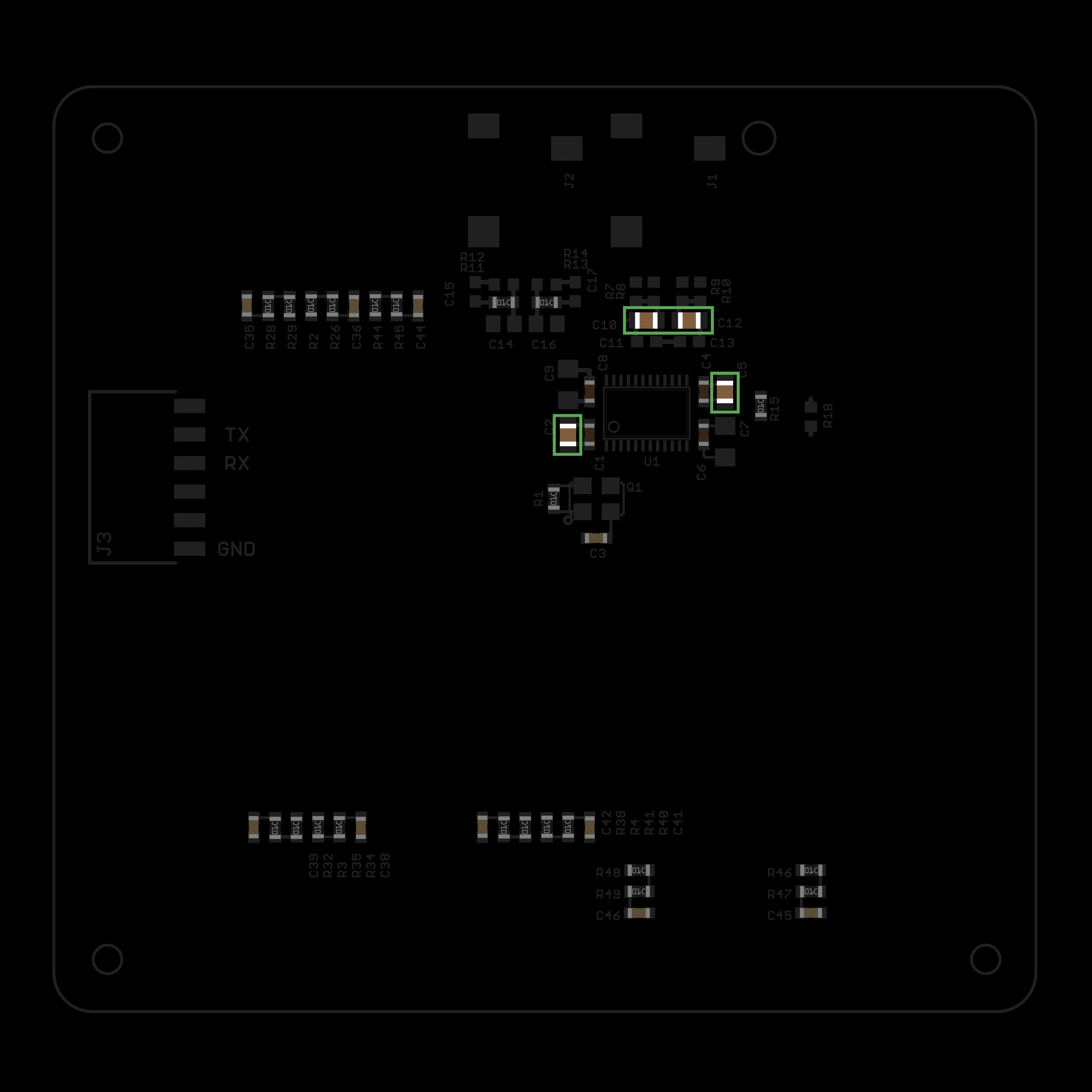
In the area indicated in GREEN place:
10uF Capacitors (MFG P/N GRM21BR61E106KA73L, brown in color)
C2 C5 C10 C12
These components can easily be confused with the similarly shaped C14 and C16, so confirm the part number.
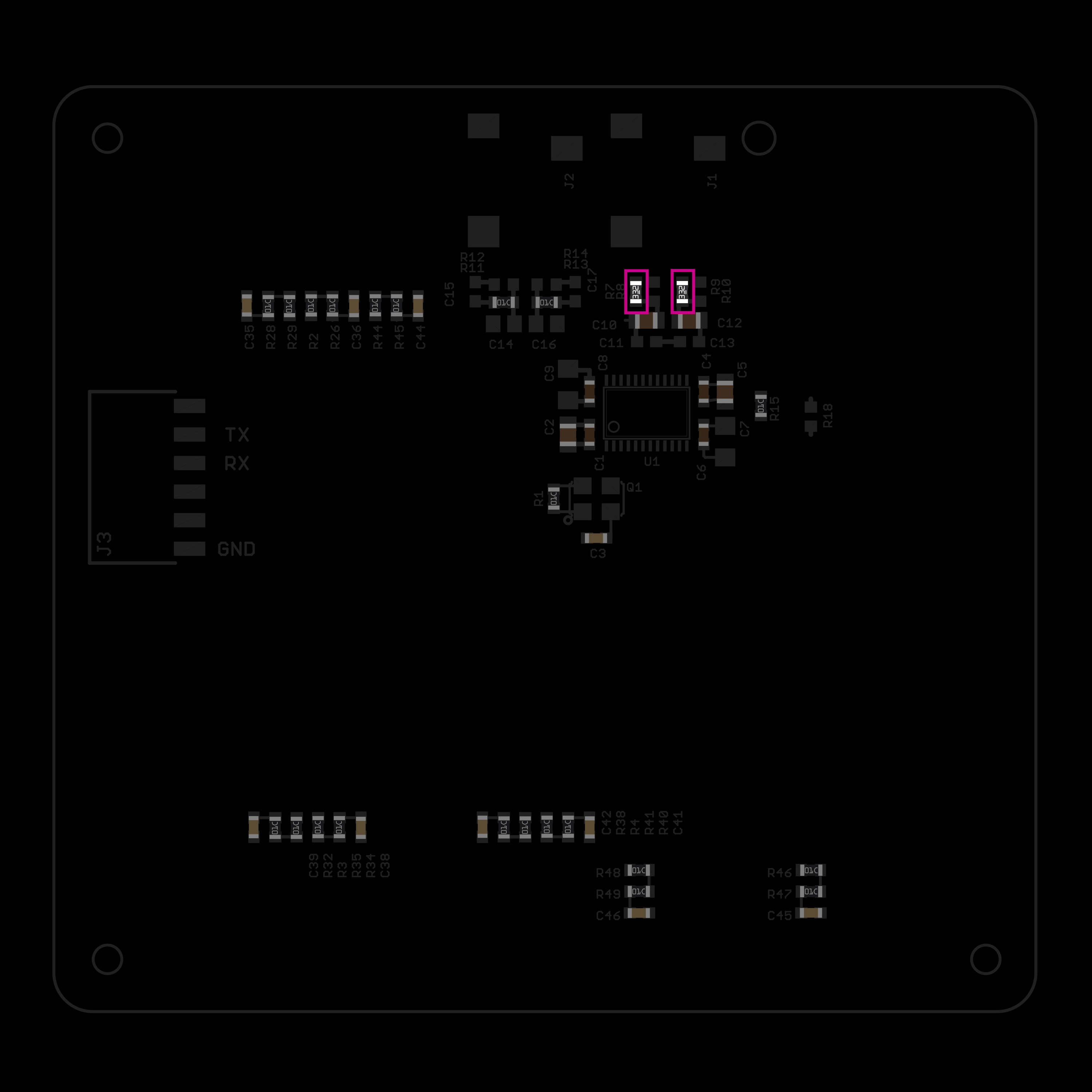
In the area indicated in PINK place:
3.3k Resistors (MFG P/N RC0603FR-073K3L, code 332)
R7, R9
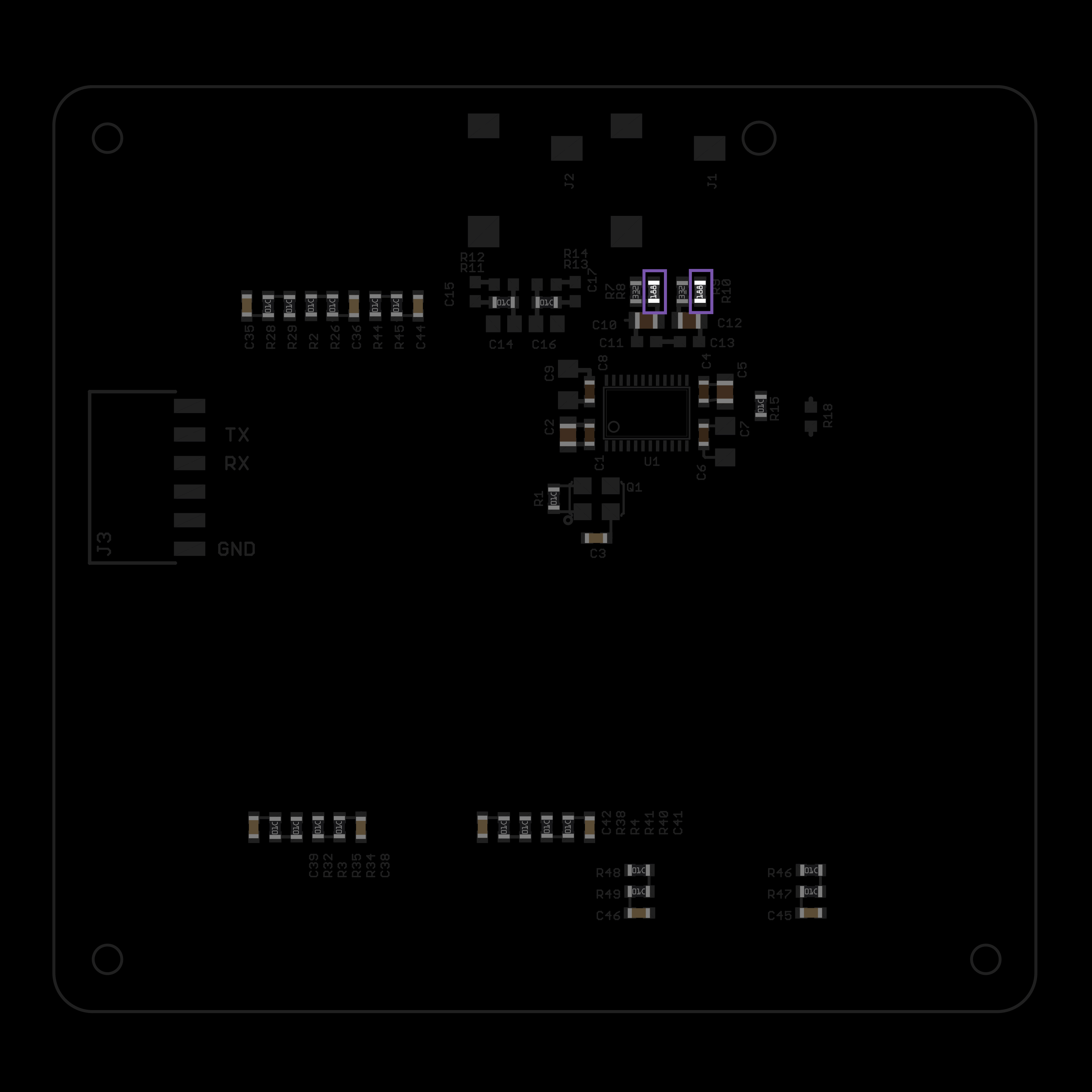
In the area indicated in PURPLE place:
1.5k Resistors (MFG P/N RC0603FR-071K5L, code 18B)
R8, R10
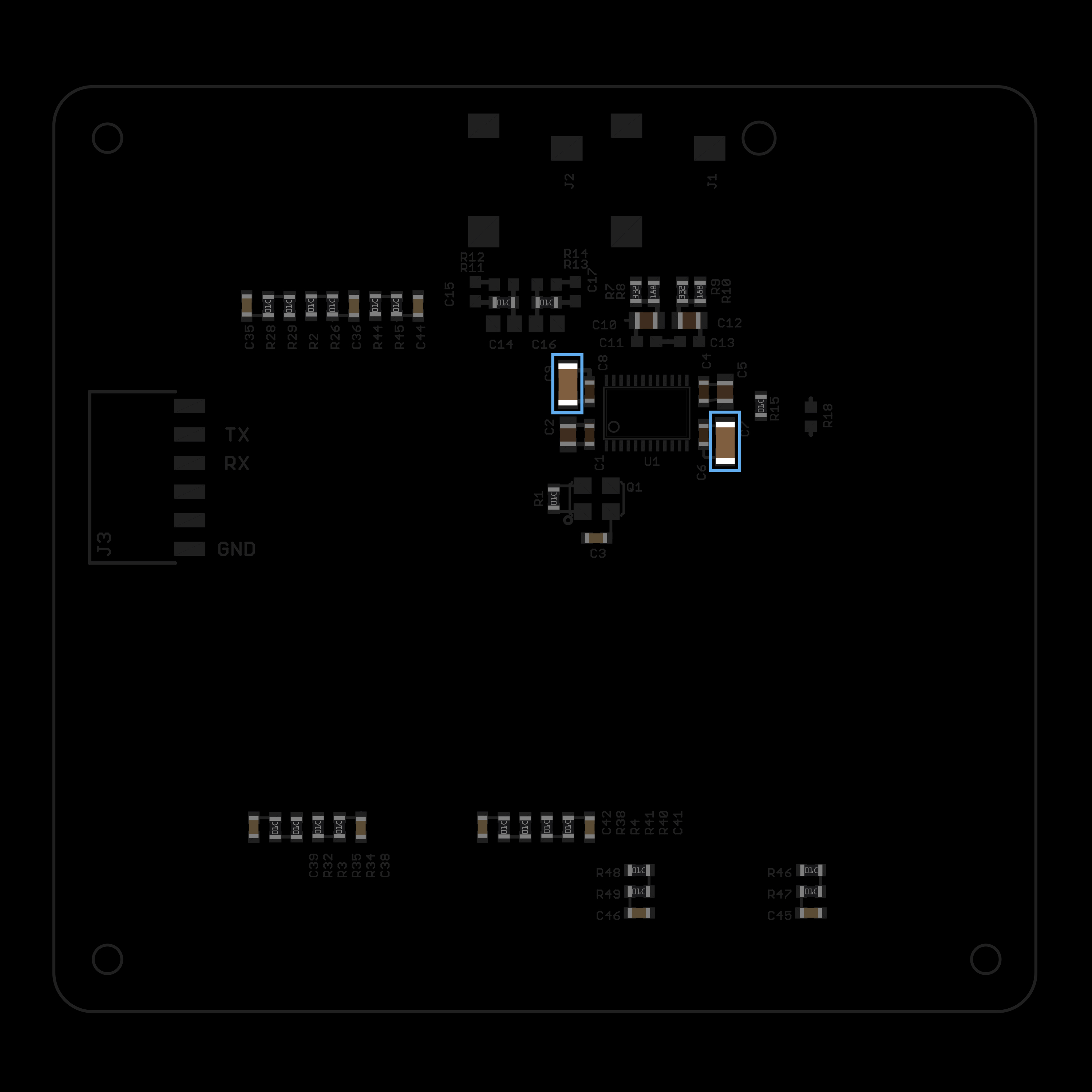
In the area indicated in LIGHT BLUE place:
47u Capacitors (MFG P/N C3216X5R1E476M160AC, brown in color, 1206 package)
C7, C9
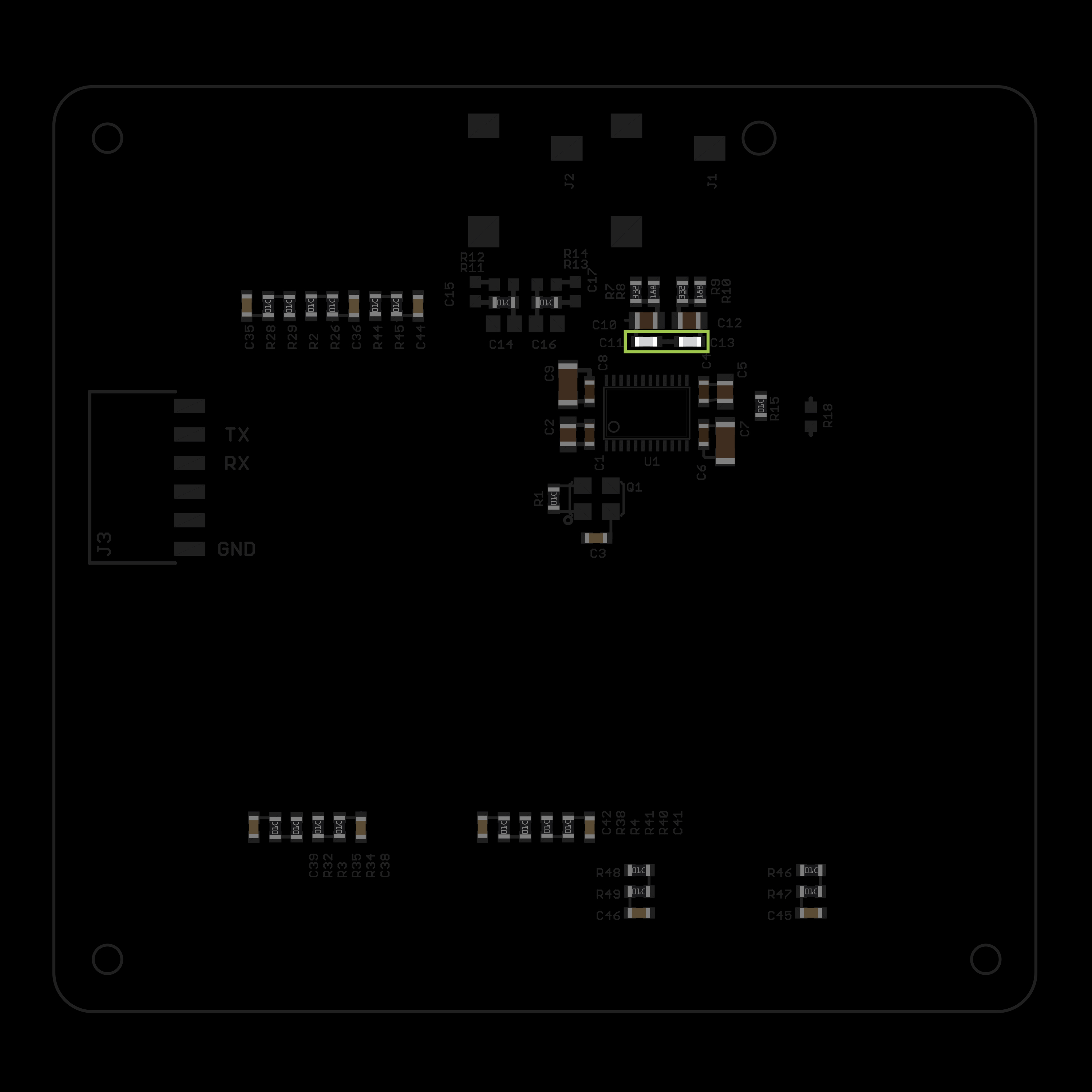
In the area indicated in YELLOWISH GREEN place:
220p COG Capacitors (MFG P/N GRM1885C1H221JA01D, greyish white in color)
C11, C13
These can easily be confused with the similar C15 and C17 so confirm part number.
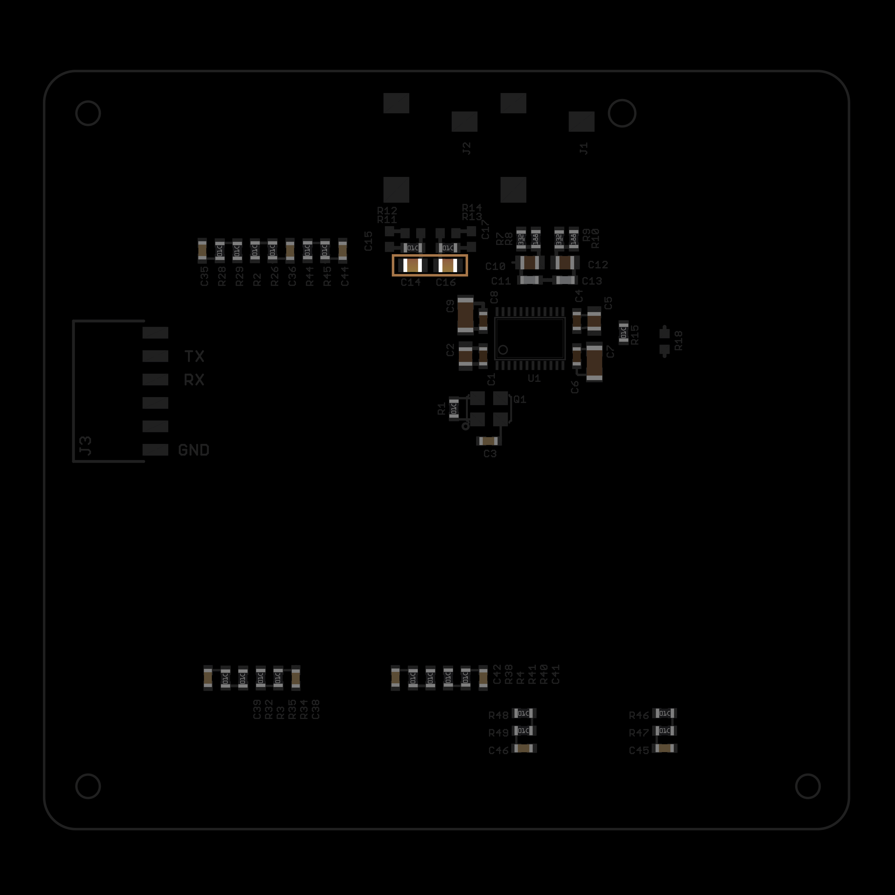
In the area indicated in LIGHT BROWN place:
3.3u Capacitors (MFG P/N CGA4J3X5R1E335M125AB, reflective brown in color)
C14, C16
These can easily be confused with the similar C2, C5, C10, and C12 so confirm part number.
C14 and C16 will have a slightly opalescent and reflective look.
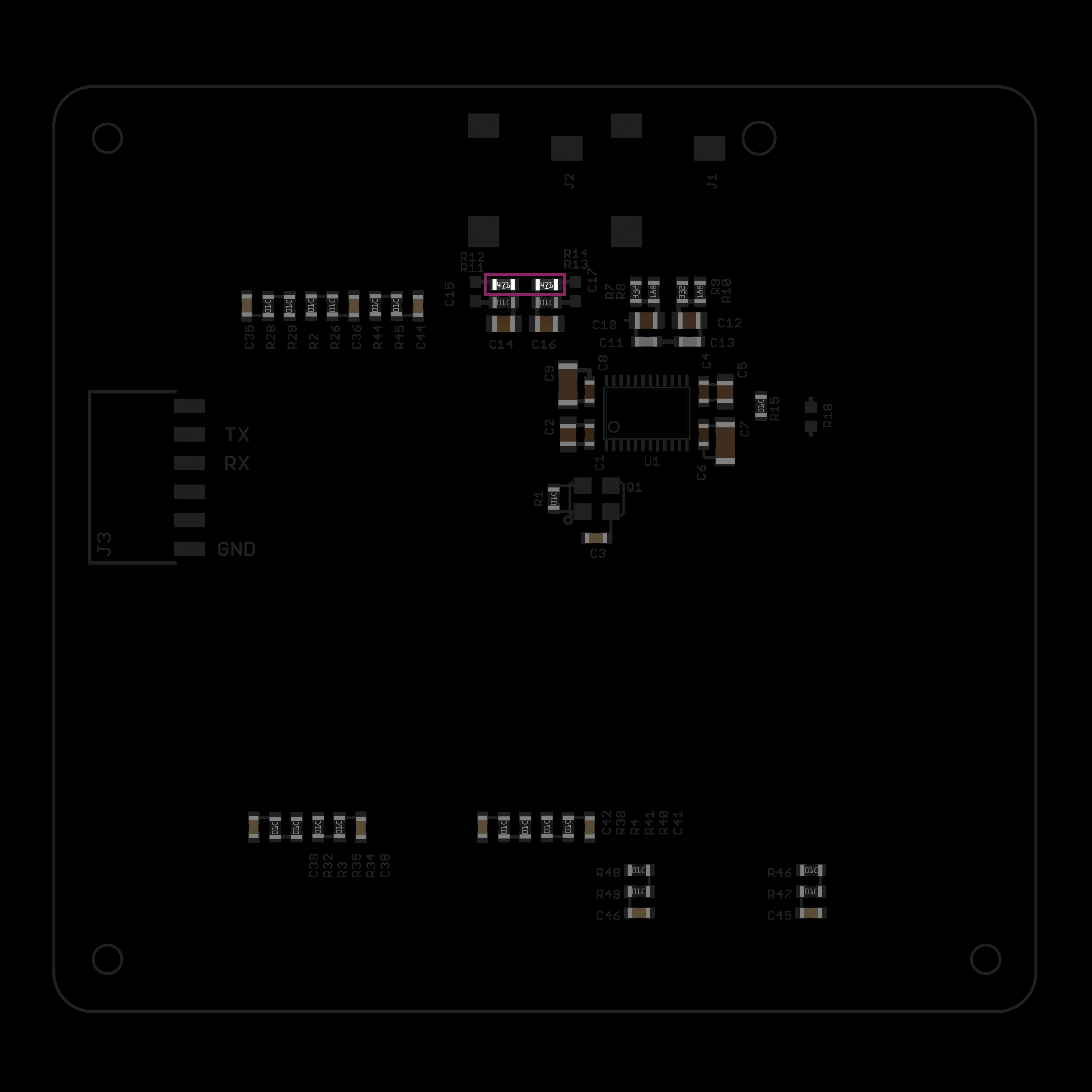
In the area indicated in FUCHSIA place:
470 ohm Resistors (MFG P/N RC0603FR-07470RL, code 471)
R12, R14
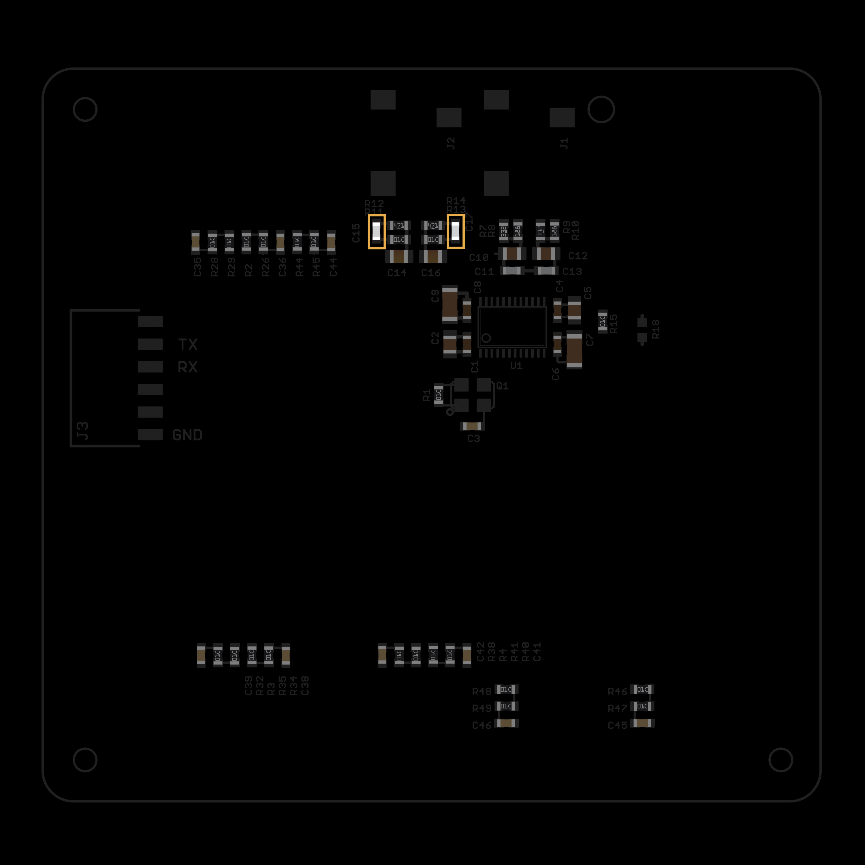
In the area indicated in LIGHT ORANGE place:
2700p COG Capacitors (MFG P/N GRM1885C1H221JA01D, greyish white in color)
C15, C17
These can easily be confused with the similar C11 and C13 so confirm part number.
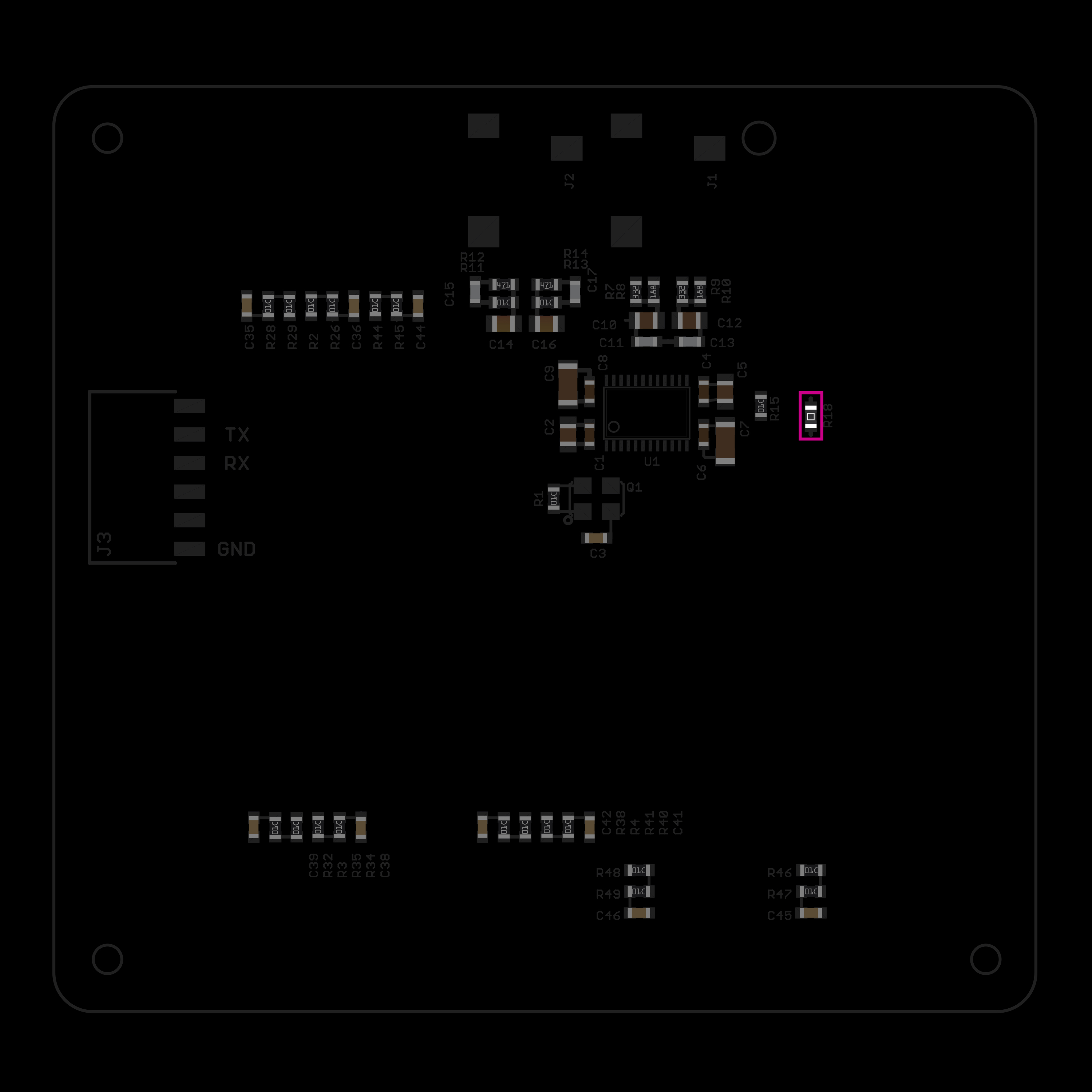
In the area indicated in PINK place
0 ohm jumper, indicated by a 0 code
You can also use a solder blob or clipped resistor lead to bridge the two ground planes.
Jumper looks nicer.
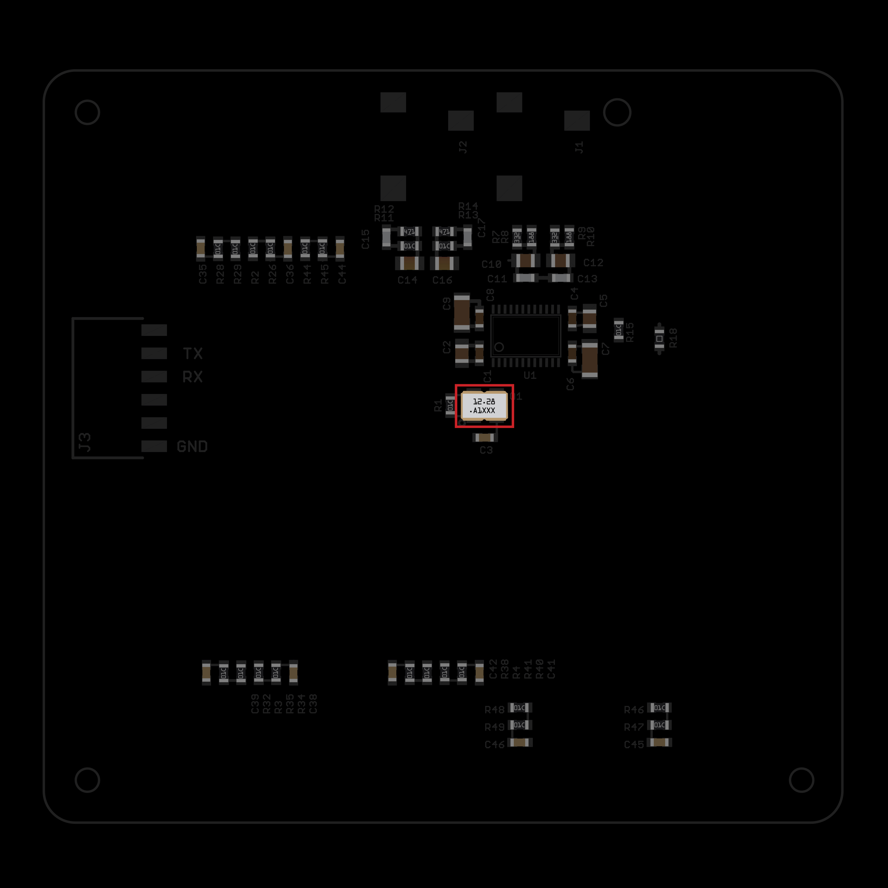
In the area indicated in RED place
ASFL1-12.288MHZ-EC-T Oscillator (Timing Crystal)
The text should be right side up if viewing the PCB with audio jacks at the top.
Putting the crystal on upside down can fry it, so double check orientation.
I recommend not putting any solder on the pads before placement. Add flux to pads, place crystal on pads, hold with tweezers and tack one pad then add solder to the outside of each pad area bridging the gap between the side of the Crystal and the edges of the solder pads.
Keep an eye on how much solder you are using and how the crystal sits on the pads. Proper placement is critical to ensure functionality. This area can also create shorts to ground that can affect the Pi operation. Check for bridges with a multimeter before moving on.
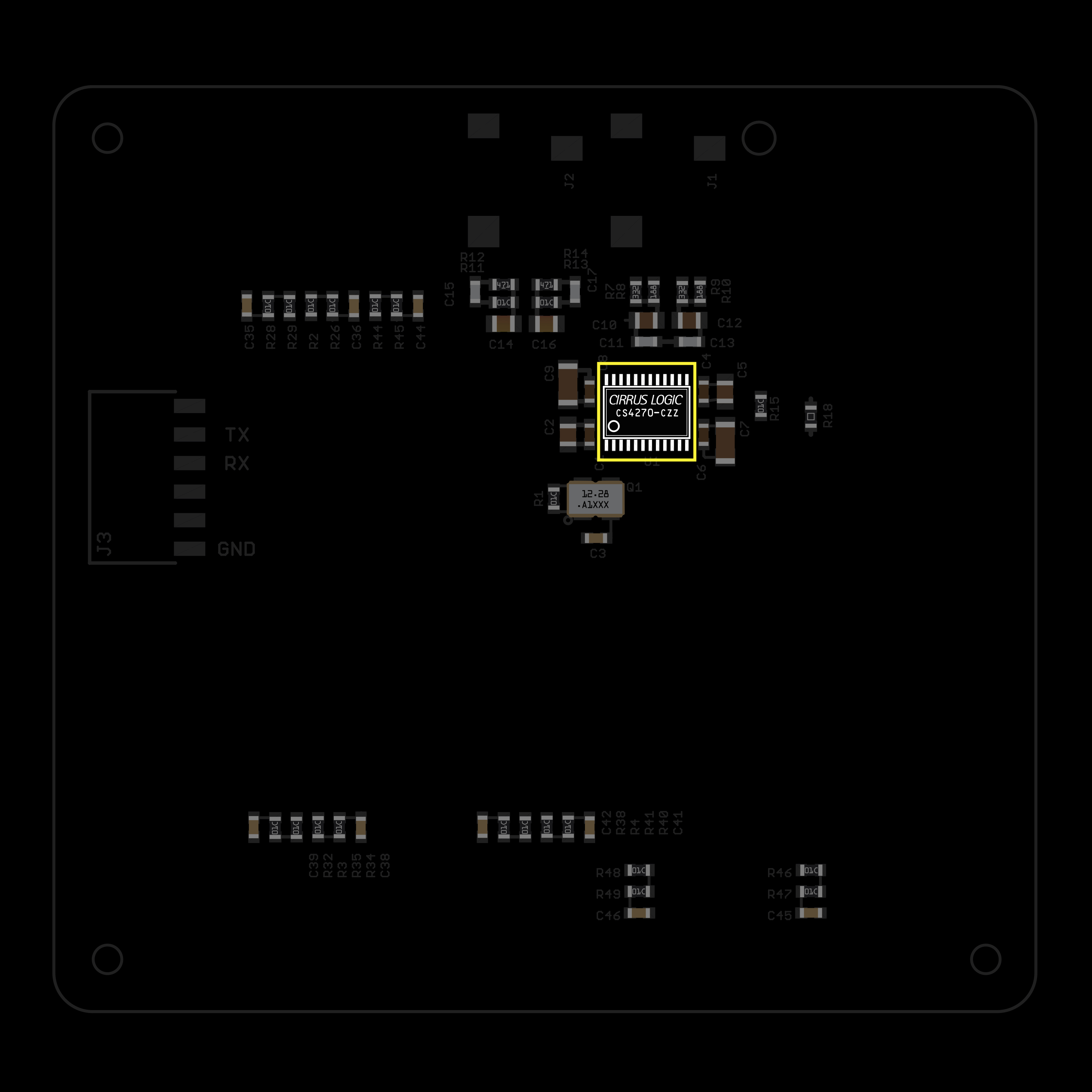
The codec is the most difficult and critical component, hence why we place this last.
These are difficult to source, they have become expensive, but most importantly of all, they are nearly impossible to remove without an SMD rework station. If you have more than one, might as well not waste a chip which you can pass onto a friend.
Same placement principle as the crystal. Add flux to pads, place chip and line up the legs with the pads, tack one leg and move it around (CAREFULLY)
Tack another leg opposite and diagonally to the first leg. Make sure everything looks nice. Add a bunch of flux (go crazy) and use the swipe soldering technique to do the rest of the pins. Watch for excess solder, add flux and swipe again.
Now you can deeply clean the board with ISO alcohol. Take special care to clean off the Codec for inspection. With magnification, look for bridges between the pins, add flux and swipe down along the pin (perpendicular to previous solder swipe) to clear bridges.
Clean and inspect. Clean and inspect.
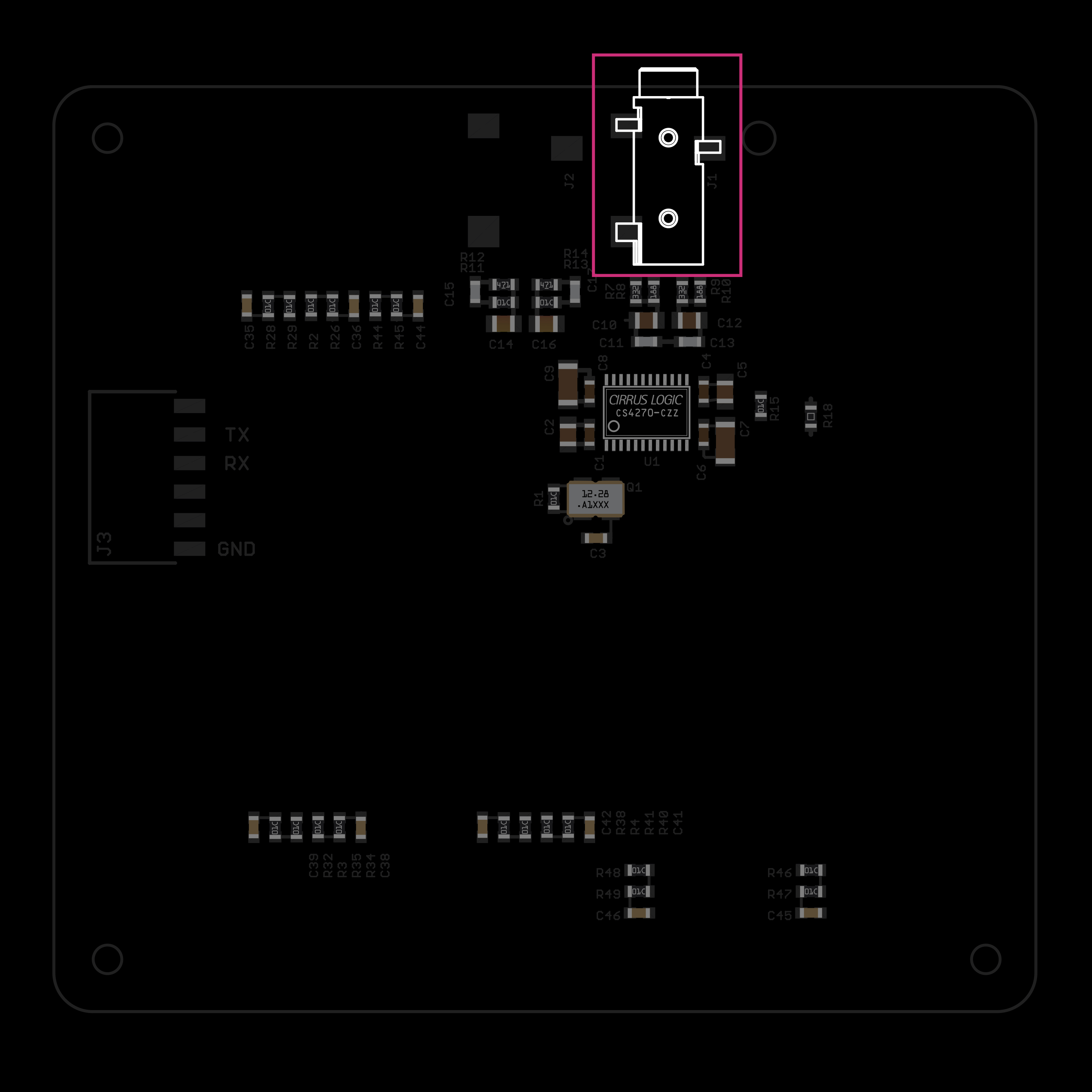
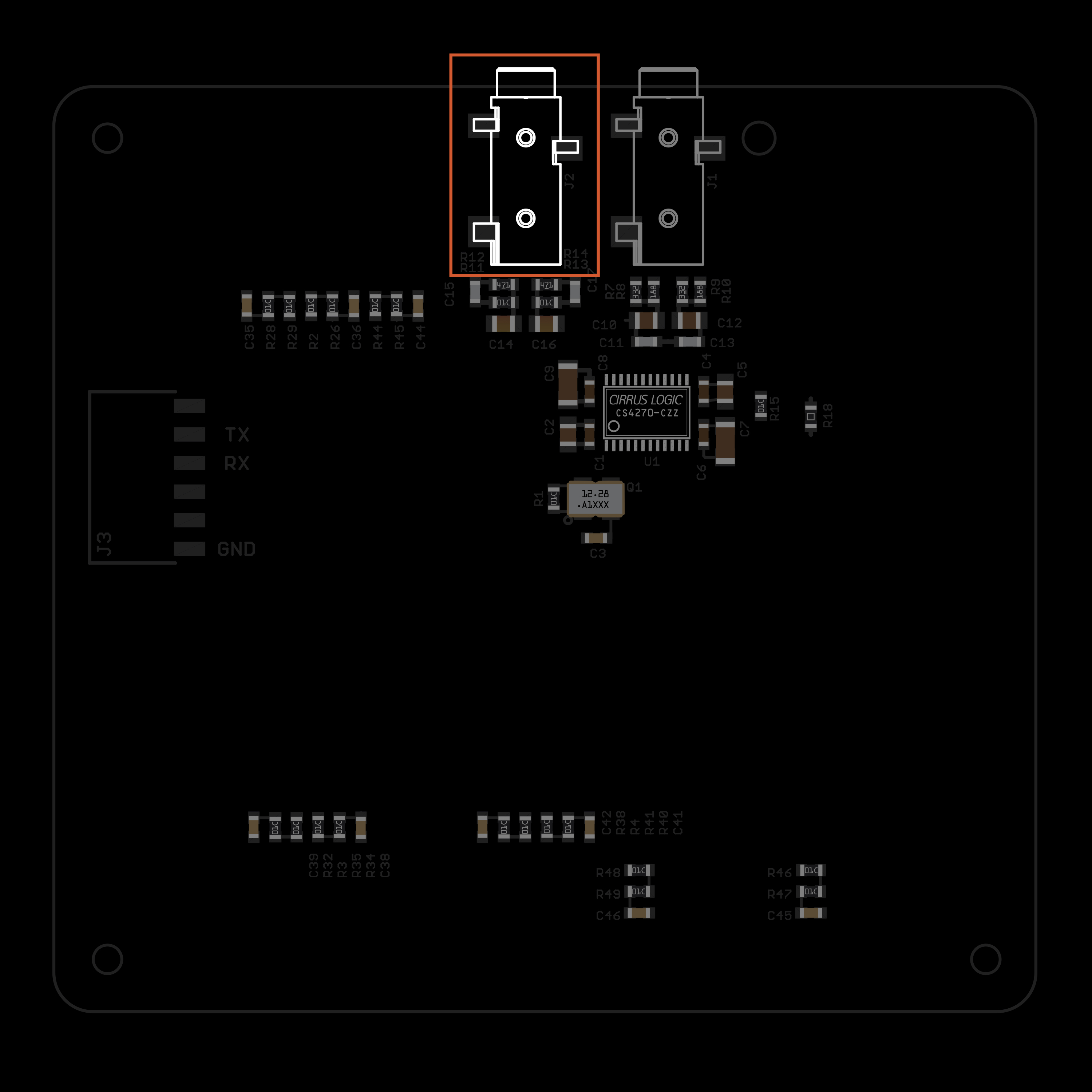
Place the input and output jacks.
I place the Input jack first (right side if looking at PCB from bottom) as it has 2 legs between the jacks. Place retainers in holes, tack one leg and move the jack around until it is straight. Tack second leg, check placement. You can still move the jack from side to side with two legs tacked by applying some heat to a joint and horizontal pressure in the direction the jack needs to go. Try to apply downward pressure so the jack lays flat.
Same process. Solder the two outside legs first and get your placement finalized. Take care soldering the leg in between the two jacks. You can easily melt a jack if you are not careful. Do this leg last to prevent having to get your iron in between the jacks more than once.
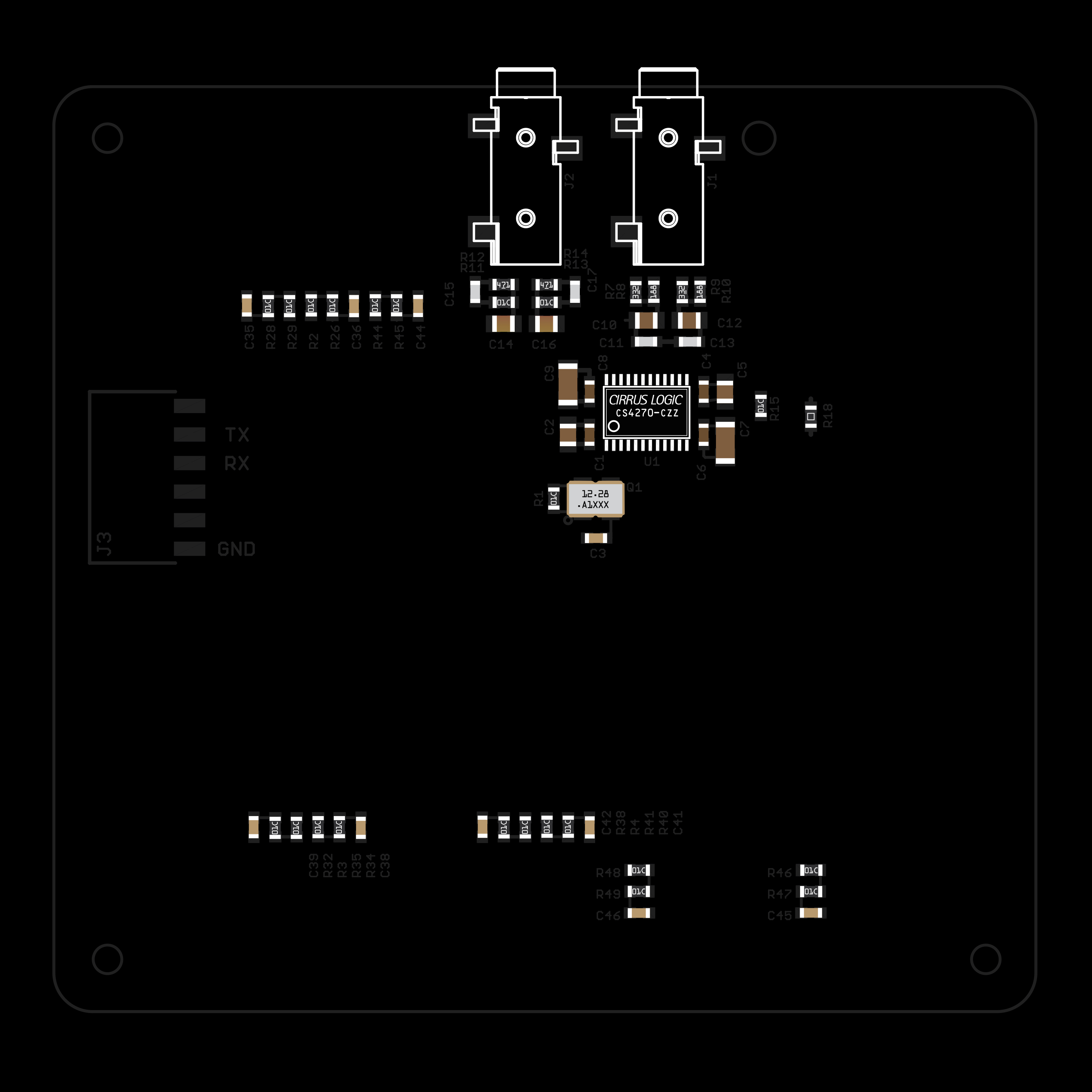
The SMD portion of the build is now complete. Clean, inspect and check each area for proper component placement.
FAQ and Troubleshooting:
Switch / Encoder not working: Check for correctly soldered and placed resistors / caps in each switch / encoder area. Check Pi header for proper soldering. For encoders, check that all the through hole pads are making connections, if you have popped a pad, you can always run a jumper wire to the proper point.
Switch / Encoder causing Pi to turn off : Usually solved (for some reason) by reseating the crystal and touching up the Pi header.
SUPERCOLLIDER FAIL : Check for bridges on Codec, check for proper Crystal placement. Reset Crystal if it is sitting to high or crooked. Touch up Pi header by applying pressure to each pin as you go, ensuring the solder flows down the pin.
Audio input / output levels stereo pairs do not match: During testing I play a song off of my phone to test the inputs / outputs of the shield. If one side is WAY off from the other, an incorrect resistor value may have made its way into the input or output path. Check values.
Non Red Light on Pi not flashing during boot: Issue with the Norns image on the SD card. Reflash card. If card is fine, this is often an issue with the Pi header as the Pi is not initializing the SD card.
Glitched image on OLED or No Image : Check display header soldering and check display for proper 3.3v on Pin 1 (left to right looking at display from top with header on bottom, Pin 2 is GND)
I'll add to this as I remember more common issues. Feel free to email me ryan@uxorio.com or PM me @alley_cam on Lines if you have any questions or suggestions.
