Yet Another GPS/PPS disciplined (opn/pf)sense thing
The core concept isn't anything "new" or "innovative" (see below) but the specific implementation is. While the implementation was specific to my needs, I'm publishing it because it may be useful for others as well.
TL;DR
My preferred router/firewall OS has a built in NTP server known as ntpd.
Precisely how NTP works is beyond the scope of the document, but in short:
- The more time sources available to
ntpd, the more accurate the local time will be. - GPS is an incredibly accurate time source.
- Most GPS receivers can also output a "pulse per second" signal to further minimize drift in clock between the GPS time updates.
When you combine a GPS/PPS signal with many other time sources, you get an incredibly accurate local time source with astoundingly low jitter.
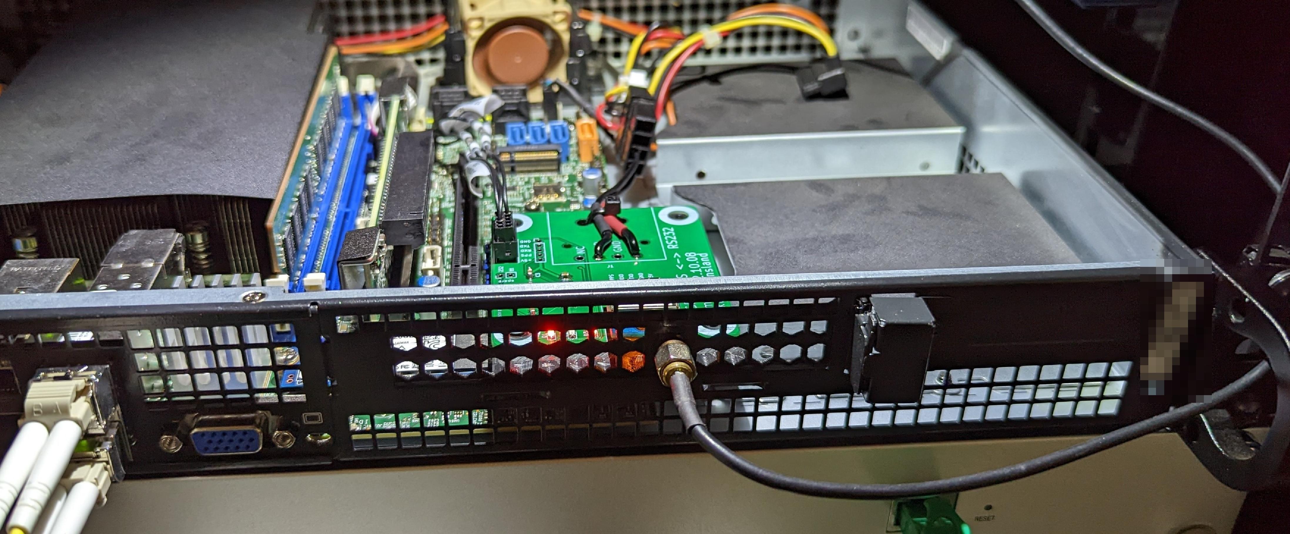
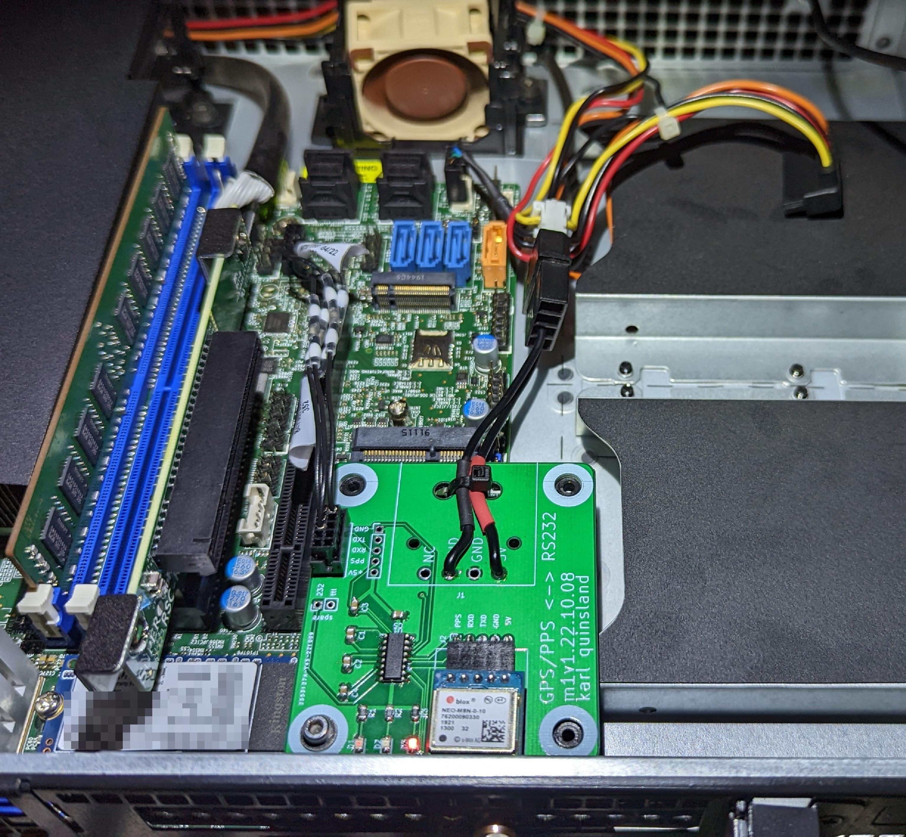
This is a simple project that allows me to integrate a commodity GPS receiver module directly into the chassis that my router/firewall host runs in.
- Yet Another GPS/PPS disciplined (opn/pf)sense thing
- TL;DR
- Overview
- PCB
- Note:
PPSpin - Note: Supermicro and generic
- Note:
sparepins - Issues
- Issue: Pin 1 for the level converter chip is not clearly marked
- Issue: mounting holes in PCB are too large
- Issue:
RXDandTXDare confusing - Issue: Some converter ships do not have internal pulldown resistors which results in overheating
- Issue: The (optional) LEDs on the PCB are not labeled
- Issue: The power connector for the PCB
- Note:
- PCB
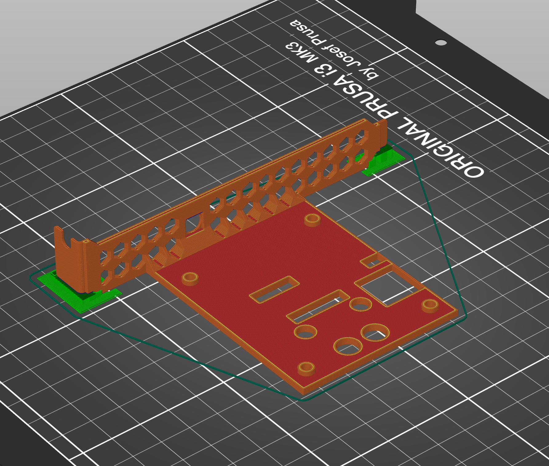
- Print the bracket
- Assemble
- Testing
- Results
- License
Prior Work
This project is based off of several existing projects / guides / posts / threads ... etc:
- GPS with PPS mod for NTP Timeserver DIY -HomeSeer Message Board
- An NTP Stratum-1 clock using a GPS 18 LVC and FreeBSD
- PFSense NTP Server With PPS DIY | IP Cam Talk/
- Building a GPS Time Reference for NTP on pfSense - YouTube
- Services — NTPD — Serial GPS | pfSense Documentation
- Network Time — OPNsense documentation
- GPS-based NTP server feature : OPNsenseFirewall/
- NTP Serial GPS with PPS signal | CocoonTech.com
- juststephen - GPS NTP with pfSense
Overview
This entire project is made up of 3 components:
- The GPS receiver module: The module I am using is the
NEO-m8nvariant of this. - The PCB that interfaces the TTL levels to the RS232 levels that my motherboard expects
- A 3d printable bracket to hold the PCB in a standard PCI card slot.
PCB
It's a pretty simple PCB that can be soldered up in less than an hour... and that includes plenty of time spent looking for where I put some of the components!
Despite the simplicity, there are a few things that I want to call attention to.
Note: PPS pin
The PPS signal is sent over the RS-232 pin 1 (DCD).
I don't know where/if/how you'd configure ntpd to check a different pin for this signal; I can't find anything obvious in the opnSense/pfSense documentation about this.
The other schematics / designs / implementations that I referenced above all use pin 1 for PPS so I just went with the convention.
Note: Supermicro and generic
The PCB was designed for my motherboard (X11SDV-8C-TP8F) which specifies a CBL-CDAT-0605 part number to break out the on-board header to a regular DB9 port.
If you google that part number, you'll find that the specific cable is not common or cheap.
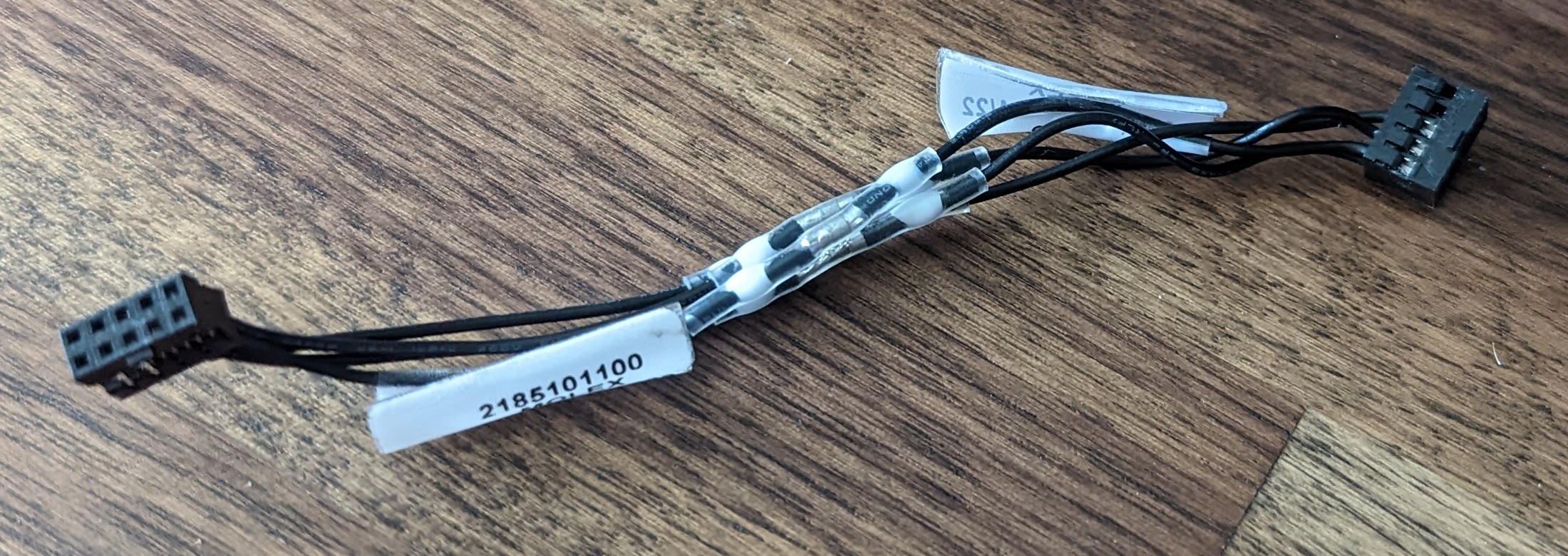
After a bit of sleuthing, I was able to figure out that the connector on the motherboard is a 2x5 version from the Molex MiliGrid family.
I hate crimping cables so I placed an order for 2x pre-made cable pigtails with the intent of just adding whatever length of wire was necessary.
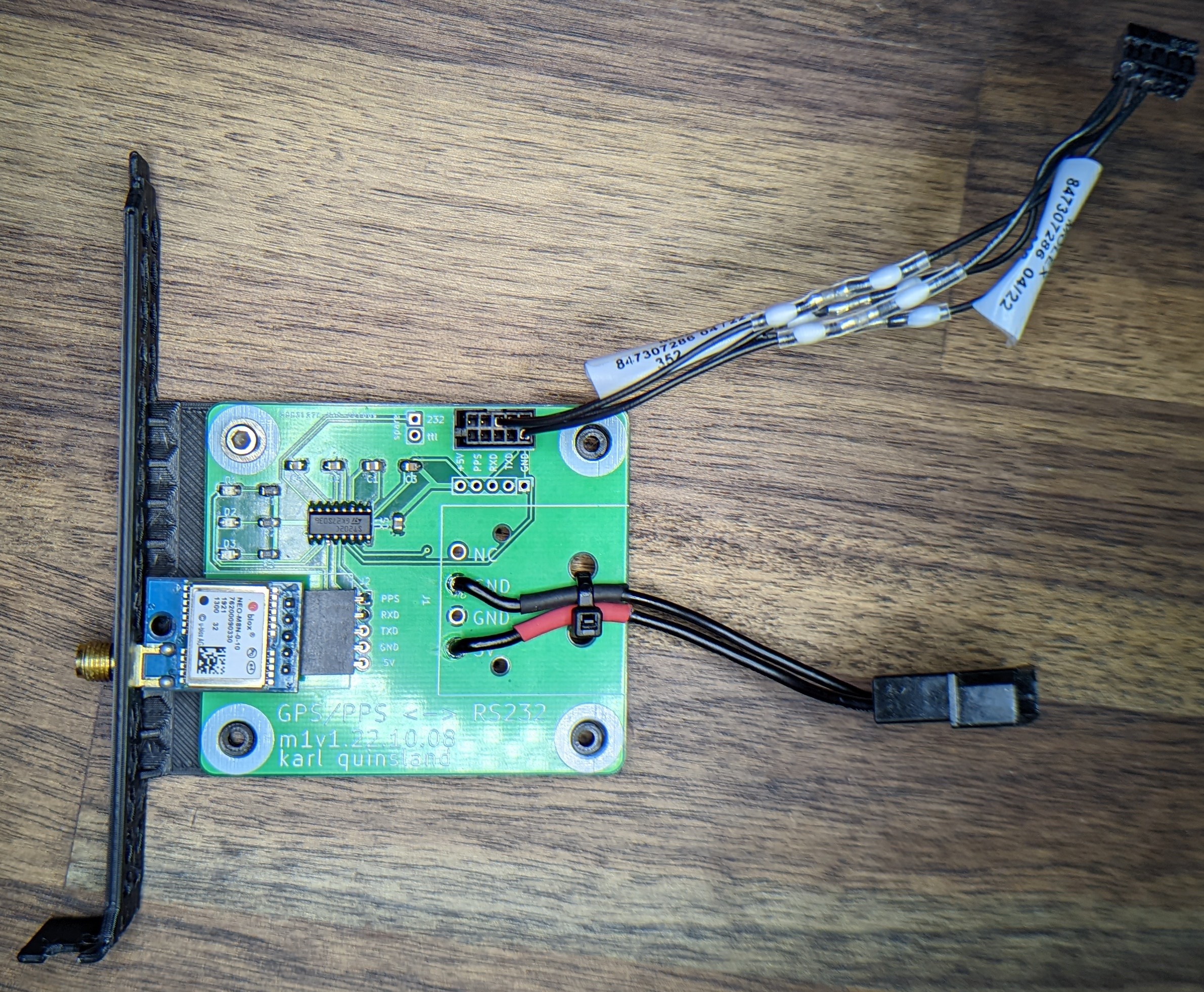
As it turns out, the 50mm cables are just long enough so just soldered the two pig tails together and then removed the extra / unneeded wires.
Close up, the cable looks like this:
To make this PCB usable in other cases, there is a generic pin header that breaks out the required signals to a standard pin header that can be adopted to work with whatever other connector/adapter is necessary for your use case.
Note: spare pins
The level converter chip technically has 4 "channels" and I only need 3 channels,
There is a small pin header labeled spare which is broken out should I ever need it.
Issues
As is tradition, the nanosecond I got the "your order is in production" message, I noticed a few things on the PCB that should be improved. While doing the initial assembly, I compiled this list of improvements and other deficiencies that should be improved in a second version.
Note I am not going to do a second revision of the PCB. While not perfect, the first revision works and I need this project off of my todo list. Rather than spend time revising the PCB and then additional time/$ waiting for the rev2 PCBs to show up, I figured it would be better to spend a fraction of the time cleaning up my notes and shipping rev1 so people decide if they want to follow the workarounds or contribute their fixes.
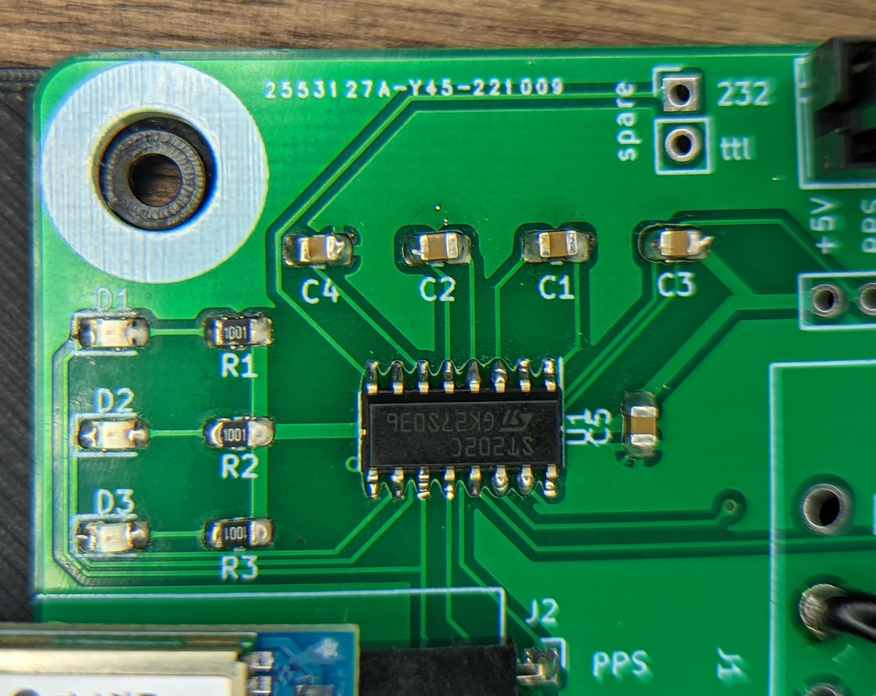
Issue: Pin 1 for the level converter chip is not clearly marked
Fortunately, the interactive BOM / PCB layout tool has you covered! If in doubt, just make sure that your chip has Pin 1 attached to the pad that faces C{1,3,5} as shown here:
Issue: mounting holes in PCB are too large
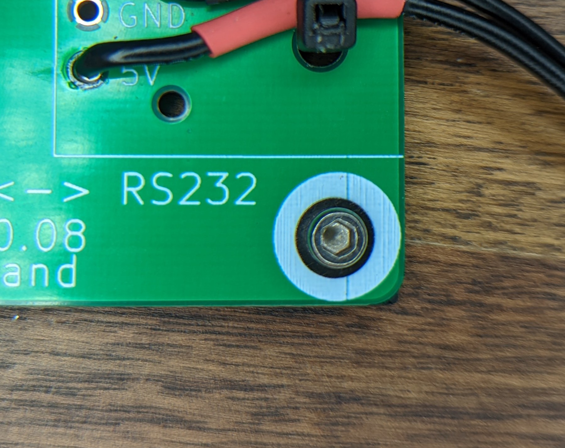
The four holes on the corners of the PCB were meant for m3 screws. I'm not sure what happened, but somehow the diameter of the holes is about the size of a typical m3 screw head.
You can work around this with a simple washer as shown below. Additionally, if you're not going to use the PCB mount power connector, a ziptie will keep the PCB in place
Issue: RXD and TXD are confusing
I'll spare you the rant, but these standard names are so poorly chosen it's not even funny. Basically, I mirrored the pins from my motherboard on the PCB and that resulted in the GPS module transmitting into the motherboards transmit pin as well.
To save some trouble, the PCB could be updated with a simple cut-trace/solder jumper block for creating a "cross over" connection on the PCB.
I was able to work around this by just swapping the rx/tx pins on one side of the cable.
It would have been nice to not need to modify the cable and just do this by moving a solder blob on the PCB.
By breaking out the pins on the PCB, you'd also gain some test points which would make debugging a bit easier.
Issue: Some converter ships do not have internal pulldown resistors which results in overheating
It's 2022 and there's a chip shortage. In fact, in the ~72h gap between picking parts and submitting the PCB for production, the original chip I selected went out of stock! Fortunately, there are a zillion pin/footprint compatible ICs that are drop-in replacements so I got lucky!.
It should be noted that some of the max3232 equivalent chip have built in pull down resistors on the TTL inputs. This is especially true with the counterfeit chips that are commonly available. When the input is left floating, the circuit can "latch up" into a short circuit which results in the chip RAPIDLY getting very hot.
The particular IC that I chose (ST202CDR) has internal pull downs but it would have been trivial for me to add a few optional resistors to the schematic.
If you end up using this PCB with a chip that does not have the internal pull downs, you'll want to add your own with a bodge wire!
Issue: The (optional) LEDs on the PCB are not labeled
D{1,3} are optional LEDs that blink when there is activity on the RX, TX or PPS pin.
If you look at the gerber files submitted to the fabrication house, there is a silk screen label for each LED... but for some reason the labels didn't get printed.
Issue: The power connector for the PCB
As of this writing, the PCB was designed with a PCB mount version of the 4 pin computer power supply connector (formally known as AMP 1-480426-0, apparently).
Unfortunately, the part that I ordered did not arrive in time and the seller was not able to provide useful documentation for dimensions so the PCB footprint is a complete guess.
This is why you see a pigtail soldered on to the PCB instead of an on-pcb socket.
Any source of 5v will work, you don't need to use the connector that I've shown in the photos!
Print the bracket
Speeds and feeds are up to you; some cases are much more forgiving of an "out of spec" PCI card and others - like mine - are not. Print as slow as needed to get as precise as needed.
Using PLA and my tweaked ".2mm / quality" setting with a .6mm nozzle took about an hour.
Only time will tell if PLA was an inappropriate choice for inside of this server. I'd like to think that the ventilation and cooling are sufficient but I might be re-printing the bracket in ABS if I notice any warping.
Note For best results, you'll need a TINY amount of support material (shown in green above) for the ends of the PCI blank that are not flush with the print bed.
Additional files
I've also included models of the GPS module and PCB in STEP format should they be useful in creating an alternate enclosure or application
Assemble
This is pretty straightforward.
Use the interactive BOM / PCB layout tool if you have questions. If your question isn't answered there, the KiCad project files should have you covered :D.
When done, it should look something like this:
Testing
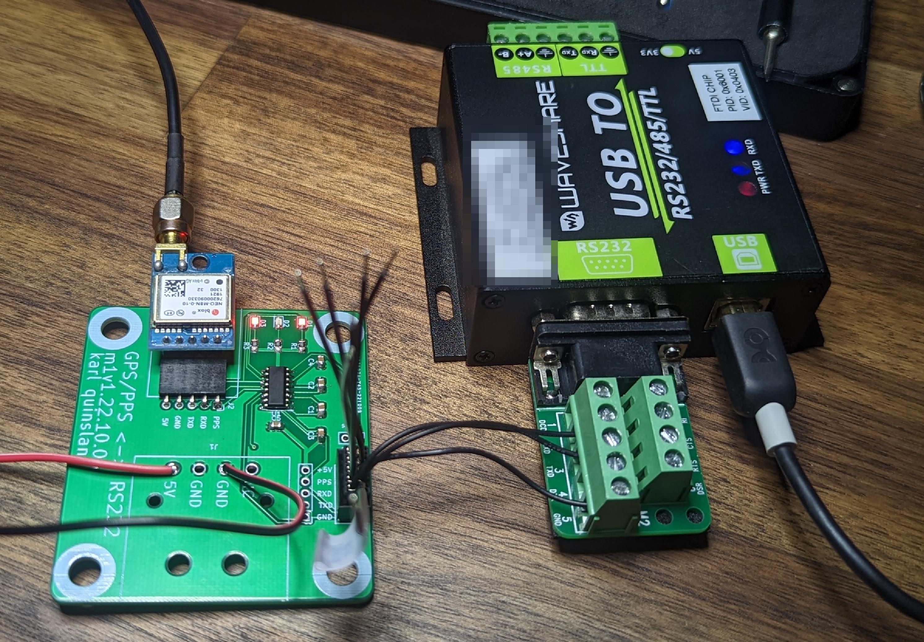
Pro tip: test your cheap hand made electronics before integrating them into your expensive and "critical path / production" computers.
Using a terminal program, I could see valid packets coming in. This told me that the lever converter was working and the RS232 <-> USB converter was happy with the levels.... a good sign!
After installing into your system, you can use a serial modem terminal application to verify data coming in or to check which serial port data is coming in on.
Opnsense has the cu binary installed and can be used like so:
root@opnsense:~ # cu -l /dev/cuau0 -s 9600
Connected
$GLGSV,<..........>*69
$GLGSV,<..........>*65
$GNGLL,<..........>*61
$GNRMC,<..........>*7C
<...>
$GNVTG,<..........>*35
$GNGGA,<..........>*76
$GNGSA,<..........>*17
$GNGSA,<..........>*1D
Note I've stripped out the NMEA sentences and replaced them with
<..........>but rest-assured, I did check the reported coordinates and they were accurate.
Results
It takes a moment for the GPS module to acquire a fix and start sending location data to ntpd but after a few moments, the ntp stats settle down:
me@opnsense:~ # ntpq -p
    remote           refid      st t when poll reach   delay   offset  jitter
==============================================================================
xGPS_NMEA(0)     .GPS.            0 l   15   16  377    0.000   -0.006   0.001
<...>
-66.85.78.80     172.16.23.153    2 u   43   64  377   61.986  +100.12   0.339
*time4.google.co .GOOG.           1 u   37   64  377   47.039  +103.78   1.048
-40.119.6.228    25.66.230.2      3 u   42   64  377   42.901  +102.38   0.583
<...>
Just look at that (lack of) jitter :D
License
Other than the content of the data-sheets directory, all files in this repo are licensed under
CC BY-NC-SA 4.0 license which permits:
    BY: Credit must be given to you, the creator.
    NC: Only noncommercial use of your work is permitted. Noncommercial means not primarily intended for or directed towards commercial advantage or monetary compensation.
    SA: Adaptations must be shared under the same terms.
