- Overview
- FPGA Utilization
- Warnings
- Installation
- Run
- Design Breakdown
- Specifications
- Customize
- Potential Enhancements
- Known Issues
Electronic hobbyists, makers, and engineering students need low-cost and effective tools. One of these tools includes a logic analyzer for debugging digital designs. Unfortunately, there is a large gap in this market, professional grade logic analyzers start at a minimum of 400 dollars while the cheaper version is around 15 dollars but is extremely limited in functionality. There are no mid-tier options that meet the needs of the aforementioned. This project is an open-source design using FPGAs offering great performance. In addition, the design uses only Verilog source code, no IP cores or device specific features. This makes the design portable to any FPGA, you can adjust the number of input channels and memory depth very quickly. For the accompanying desktop application, Python is used to allow the GUI to work on most operating system.
- Caution: Connecting one or more of the input channels to voltages outside the range of your FPGA, even for a very short time, can result in permanent damage to either device.
- The input channels of the FPGA are not electrically isolated from each other, nor are they isolated from the PC.
- Be aware of ground loops! Read more about it here
| Manufacture | Family | Device | Frequency | WNS | LUT | FF | Channels | Memory Depth |
|---|---|---|---|---|---|---|---|---|
| Xilinx | Artix-7 | xc7a35tcpg236-1 | 100MHz | 4.313 | 198 | 223 | 8 | 4096 |
| - | - | - | - | 4.271 | 201 | 228 | 8 | 8192 |
| - | - | - | - | 4.098 | 200 | 240 | 16 | 4096 |
| Xilinx | Spartan-7 | xc7s15ftgb196-1 | 100MHz | 3.917 | 197 | 219 | 8 | 4096 |
| Altera | Cyclone IV | EP4CE10F17C8N | 50MHz | 10.729 | 404 | 238 | 8 | 8192 |
| Lattice | iCE40 | LP8K | 16MHz | x | 665 | 234 | 8 | 8192 |
- Python 3.6 or higher is required to run the GUI. Required Python packages:
- matplotlib: version >= 3.2.0
- tkinter: version >= 8.6
- The FPGA development tools vary depending on the manufacture.
- Xilinx -> Vivado
- Altera -> Quartus Prime
- Lattice -> icestudio or Icecube2
-
Launch the GUI by running:
$ python3 gui.py- Make sure that the
config.jsonis in the same directory asgui.pybefore running and that it has values for each of these fields:clk_freq,mem_depth, andnum_channels. Those fields are required and are explained in Specifications section of this README.
-
Top tool bar
- File:
- Open: Loads a configuration file.
- Save As: Saves the current settings to a configuration file.
- Exit: Closes the program.
- Capture:
- Start: Starts a capture with the current settings.
- Stop: Stops a capture, if a trigger event occurred then the data that was recorded is sent over.
- Open: Loads a saved waveform and displays it.
- Save As: Saves the current waveform to a binary file.
- Settings:
- Serial Ports: Selects which serial port the logic analyzer is connected to.
- Help:
- Has a link to the GitHub repository.
- File:
-
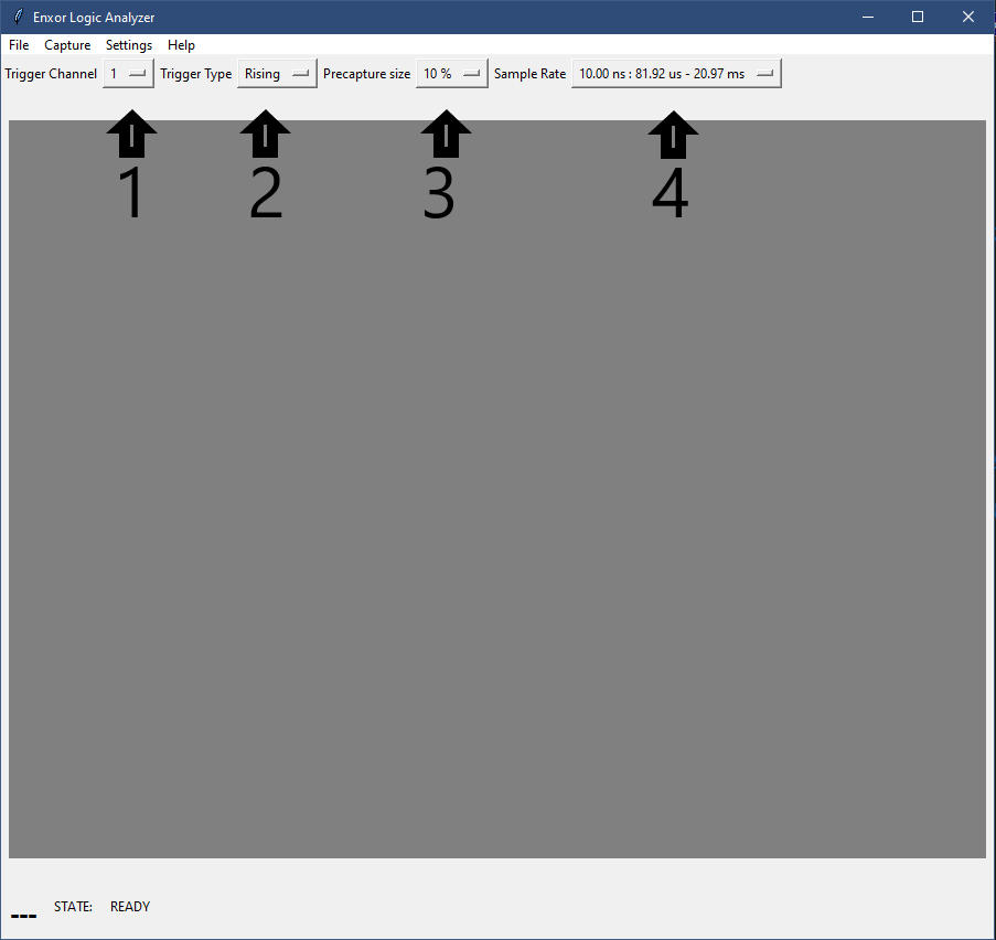
Main menu caputre buttons
- 1: Selects which channel to watch for a trigger condition.
- 2: Sets if the trigger type is a rising or falling edge.
- 3: Sets the ratio of data that will be before a trigger event.
- 4: Sets the sample rate, first number shows the sample interval rate, the next two numbers show the minimum and maximum record time respectivley.
-
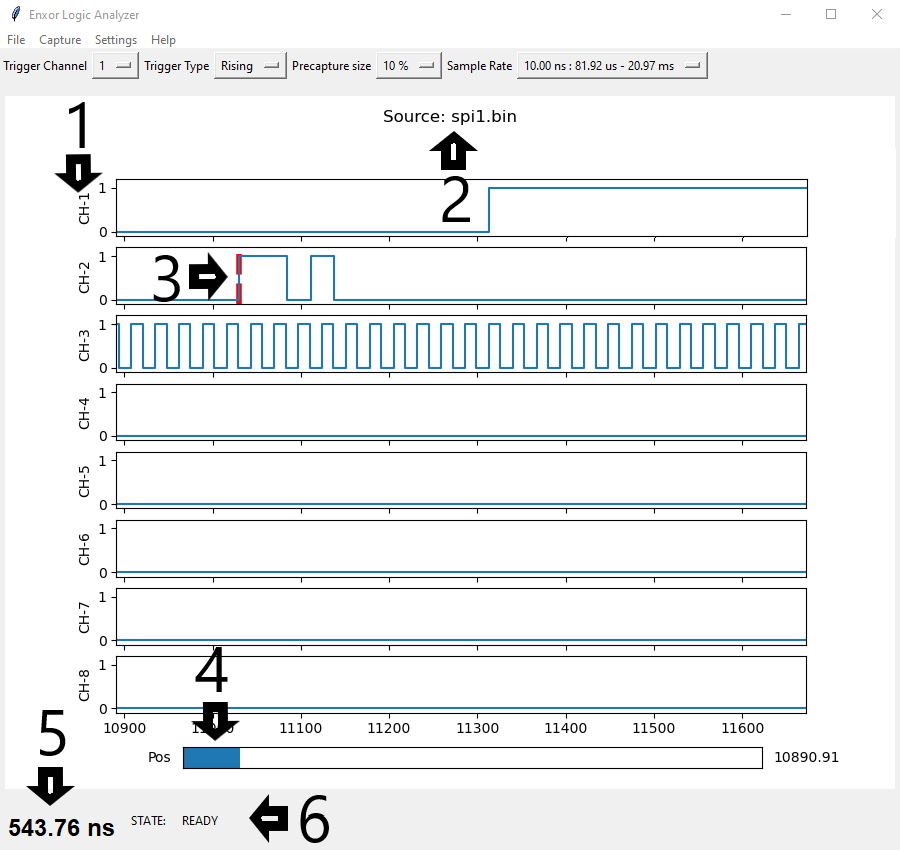
Waveform Window
- 1: The channel name.
- 2: Indicates where the data came from. Is set to the filename if loaded from one or is Enxor if the data came directly from the logic analyzer.
- 3: The red bar indicates where the trigger point occured.
- 4: The position slider controls the x-axis. Click-and-drag to move the slider to a new location.
- 5: Time measurement with units. Click anywhere on the waveform and then click on a second point to show the time between the two points.
- 6: Indicates the status of the logic analyzer. The
READYstatus indicates that the logic analyzer is ready to start a capture. When the logic analyzer is enabled but has not triggered yet, the status will beWAITING. After a trigger event, the status will beTRIGGERED. If you stop a capture in the middle then the status will beSTOPPED.


This project consists of 7 major blocks to carry out a functional logic analyzer: a trigger controller, sample rate counter, memory buffer, control module, and UART communication.

-
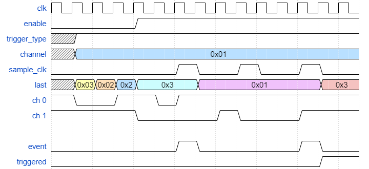
This module is set to wait for a trigger condition on a user configurable channel. That condition can be either a falling or rising edge and is set in the GUI. A sample rate signal is used to tell the trigger controller when to shift new input data in. If the new data does not match the current data, then an event signal is sent out to other blocks. Once the trigger condition occurs, a triggered state signal is sent to the memory buffer.
-
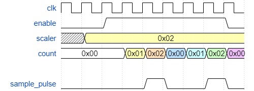
This system takes in a 16-bit divisor that tells the logic analyzer what the sample frequency should be. The sample rate signal controls how often new data is shifted into the trigger controller and how often the timestamp counter should be incremented. This divisor is needed with the FPGA clock frequency, in the GUI, to derive timing information from the relative timestamps. The sample rate signal is a pulse lasting for one clock period of the FPGA system clock, the signal does not drive the clock of any connected blocks. This helps avoid crossing clock domains as all blocks run at the same frequency.
-
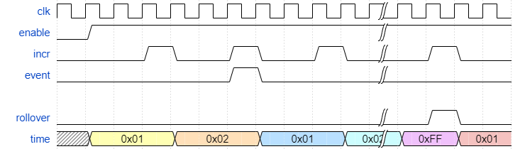
This system uses an 8-bit register to count the number of sample clock pulses. This register is concatenated together with the input data before being saved to the memory buffer. The timestamp counter is incremented at every sample clock to keep track of the relative time between events. If an event occurs the counter is reset to 1 and resumes counting. If the counter overflows, a signal is raised for the memory controller to start a new entry in the buffer. An enable signal is used to hold the counter at 1 until a capture has been started.
-
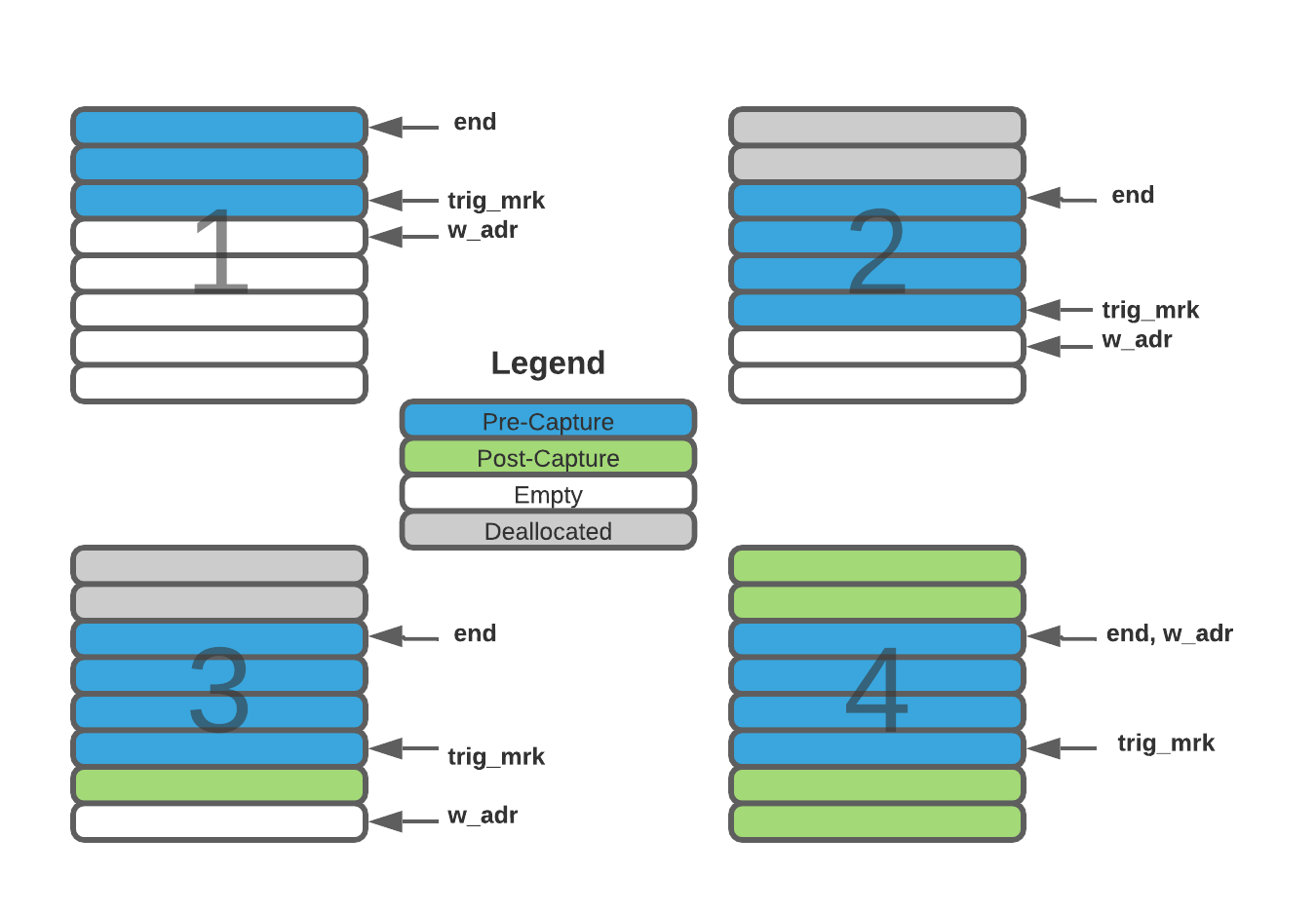
The memory buffer combines the timestamp and data storing it in RAM. Each time it receives an event or timestamp rollover signal, a new row in the buffer is started. Before a trigger condition occurs, this block behaves as a circular buffer, continually overwriting previous entries. The size of this circular buffer is programmable in the GUI and is a ratio of the entire buffer from 10% to 90%. Once a trigger condition occurs, the buffer acts as a FIFO, filling the remaining memory up. Once full, the controller module is signaled, and data is read out row by row.
- This block takes the width of the memory buffer data and converts it into 8-bit chunks so that the UART module can easily send data out. The data width converter also uses full-handshake protocol to securely transfer data from the memory buffer to the UART and to wait for the serial data to send before fetching the next entry. While it converts the width, it also prepends a header on the captured data indicating if it was captured before or after the trigger event.
- This block waits for commands to be received from the host computer and saves the commands to control registers. Once the enable command is received, the controller waits for the memory buffer to fill up. Then the data is read out of the buffer and converted from its original width to a width of one byte to be sent off to the UART block.
- This block simply waits for bytes to be sent from the host PC and relays the commands to the controller block. This block is signaled from the data width converter when captured data is ready to be sent out. The BAUD rate of the serial data is set through a parameter called CLKS_PER_BIT and can be found by taking the FPGA clock frequency divided by the desired BAUD rate and then divided by 2 once more.


-
Timming
Data sent back to the host PC has a relative sample time count byte. Each time unit is equal totime_unit_in_seconds = 1 / (clock_freq/sample_divisor)
The minimum and maximun sample time in seconds can be found by the following equations.
min_record_time = memory_depth / (clock_freq/sample_divisor)max_record_time = (max_timestamp_value * memory_depth) / (clock_freq/sample_divisor)
-
Config Format
Current settings can be saved or loaded from a.jsonfile. The following table explains what each field is and if it is required.Field Description Default Required baud_rate the baud rate of the FPGA UART 115200 N port_name the name of the serial port, i.e. COM4orttyUSB0None N precap_size number of rows in the buffer that will be used for data captured before a trigger condition 4 N sample_scaler number to divide the clock frequency. Sample frequency in seconds is given by 1 / (clk_freq/sample_rate) 1 N trig_channel the channel to watch for a trigger condition 0 N trig_type specifies if the trigger condition is a rising 1or falling0edge1 N clk_freq the clock frequency of the FPGA design in Hertz N/A Y mem_depth the depth of the memory buffer N/A Y num_channels the number of input channels to the FPGA N/A Y -
Saved Capture File Format
Captures in the GUI can be saved in a JSON formate with a.xorfile extension. The following table shows the JSON format for captures. These files used to be saved as a binary file but was more difficult to deal with. JSON files are much bigger however (24 kb vs. 150 kb), but this does not really matter on modern computers.Field Description clk_freq the clock frequency of the FPGA design in Hertz mem_depth the depth of the memory buffer precap_size number of rows in the buffer that will be used for data captured before a trigger condition num_channels the number of input channels to the FPGA trig_channel the channel to watch for a trigger condition scaler the sample rate based on the clock frequency trig-point timestamp of when the trigger point occured timestamps list of timestamps (accumulating) channel-data list of bit packed channel data. Is bit masked out for graphing -
Captured data transmitted to host PC from the FPGA.
Byte Description 1 indicates if the following data is captured before or after the tigger point
Precapture =0xA1
PostCapture =0xA3N The next byte(s) is the captured data. The number of bytes is given by the number of channels divided by 8 3 Last byte contains the count of the sample clock ticks for the sampled data. The timestamps ranges are 1-255
- In the LogicAnalyzerTop moduler are parameters that allow easy customization of the design.
DATA_WIDTHThis is the number of input channels to the FPGA and must be divisible by 8, i.e. [8, 16, 24, 32]MEM_DEPTHThis is the number of rows in the memory buffer. Total bytes in the buffer isMEM_DEPTH* (DATA_WIDTH/8 + 1)
- The UART requires a parameter called
CLKS_PER_BIT. To get the correct BAUD rate the following formula is used.CLKS_PER_BIT= (Frequency of FPGA)/(Frequency of UART)- Example:
10 MHz Clock, 115200 baud UART
10000000 / 115200 = 87
- Add a small soft-core processor to make communicating with the host PC easier and more flexible.
- Add protocol decoding
- If a data capture does not contain the full memory of the FPGA, errors occur why writting the data to or from a file
- Potential fix: dynamically write or read the amount of data in the file rather than hard-coded to the size of the memory
- Status: Resolved
- If a trigger condition occurs within microseconds after being enabled, the gui cannot get the serial port open intime to catch all the data.
- Potential fix: have Enxor signal the host PC that the buffer is full then wait for a read command before sending captured data.
- Status: Resolved
- Zooming in and out can jump around quite a lot
- Potential fix: use a percentage of the left and right window x axis values to know how much to move the window in or out.
- Status: Resolved