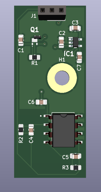
This project aims to provide a simple slow (~15KHz) but very cheap and low noise large area photodiode front end, for the use in building scientific instrumentation.
PBSS4360PA5-QX
TC1014-3.3VCT713
OPT101P-J
0805 Resistors
0805 Ceramic Capacitors
0805 Tantalum Capacitor (optional)
The general scheme of this device is shown below. As can be seen, it is formed of three sections: a capacitance multiplier, a 3.3V regulator, and the OPT101 itself. The first two stages function to minimise input noise as much as possible, with the capacitance multiplier functioning to almost entirely remove mains ripple. The OPT101 is a monolithic photodiode and single-supply transimpedance amplifier, so conveniently amplifies the photodiode output without requiring an external TIA and biases the device too. The disadvantage of course is that it has a relatively limited bandwidth of ~15KHz, but this should be good enough for applications that require only a slow response time such as a spectrophotometer.
The PCB itself can be fabricated using your favorite online service by simply uploading the "photodiode for fabrication.zip" file to their online store. I go with JLCPCB, but others are available. Assebly should also be possible using these services if you provide a BOM too, though some special considerations may need to be made for the OPT101 chip since it is an optical component. Elsewise, you can do what I did and hand solder the components.
It is an option to use a tantalum capacitor for C1 to avoid the microphonics associated with ceramic ones. The device can be mounted to a case with a M4 bolt and is designed such that it has no conductive pads on its back and the area around H1 is grounded. As such, if bolted to a conductive case, the case will be grounded and act as an EMI shield. Using only one screw hole also allows fine angluar adjustment of the placement of the photodiode, should that be required.
R2, R3, C4, and C5 are all optional and can be used to set the gain and bandwidth of the detector yourself, details on this are in the OPT101 datasheet (https://www.ti.com/lit/ds/symlink/opt101.pdf). If you would like to use the chip with its internal gain of 1M

