Arduino library for the AD7124 ADC
Copyright © 2017-2018 epsilonRT, All rights reserved.

This library allows the simplified use of both AD7124-4 & AD7124-8 analog to digital converters from Analog Devices.
Although initially intended for the Arduino platform, this library will be easily accessible on any platform with an SPI bus.
All you need to do is implement an ad7124-driver.cpp file containing the specific code.
AD7124 Library is an open source project under CeCILL Free Software License Version 2.1
The project is hosted on github.
API is documented on www.epsilonrt.fr.
To install the library, simply download its zip file and integrate it into your sketch according to explanations on the Arduino site.
Here is a simple example that displays on the serial device the voltage measured between pins AIN1 (+) and AIN0 (-):
#include <ad7124.h>

const int ssPin = 10;
Ad7124Chip adc;

void setup() {

  //Initialize serial and wait for port to open:
  Serial.begin (38400);
  while (!Serial) {
    ; // wait for serial port to connect. Needed for native USB port only
  }

  // prints title with ending line break
  Serial.println ("AD7124 Voltmeter");

  // Initializes the AD7124 device, the pin /CS is pin 10 (/SS)
  adc.begin (ssPin);

  // Setting the configuration 0:
  // - use of the internal reference voltage 2.5V
  // - gain of 1 for a bipolar measurement +/- 2.5V
  adc.setConfig (0, Ad7124::RefInternal, Ad7124::Pga1, true);
  // Setting channel 0 using pins AIN1(+)/AIN0(-)
  adc.setChannel (0, 0, Ad7124::AIN1Input, Ad7124::AIN0Input);
  // Configuring ADC in Full Power Mode (Fastest)
  adc.setAdcControl (Ad7124::StandbyMode, Ad7124::FullPower, true);
}

void loop() {
  long value;
  double voltage;

  // Measuring Voltage on Channel 0 in Single Conversion Mode
  value = adc.read (0);

  // The value is converted into voltage
  voltage = Ad7124Chip::toVoltage (value, 1, 2.5, true);
  // Print result
  Serial.println (voltage, 3);
}
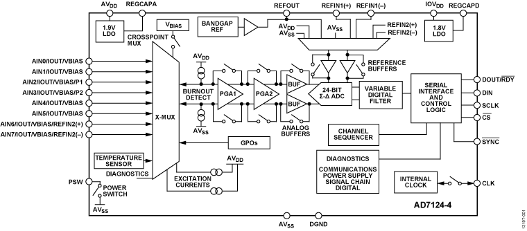
The AD7124-4 is a low power, low noise, completely integrated analog front end for high precision measurement applications. The device contains a low noise, 24-bit Σ-Δ analog-to-digital converter (ADC), and can be configured to have 4 differential inputs or 7 single-ended or pseudo differential inputs. The onchip low gain stage ensures that signals of small amplitude can be interfaced directly to the ADC.
One of the major advantages of the AD7124-4 is that it gives the user the flexibility to employ one of three integrated power modes. The current consumption, range of output data rates, and rms noise can be tailored with the power mode selected. The device also offers a multitude of filter options, ensuring that the user has the highest degree of flexibility.
The AD7124-4 can achieve simultaneous 50 Hz and 60 Hz rejection when operating at an output data rate of 25 SPS (single cycle settling), with rejection in excess of 80 dB achieved at lower output data rates.
The AD7124-4 establishes the highest degree of signal chain integration. The device contains a precision, low noise, low drift internal band gap reference, and also accepts an external differential reference, which can be internally buffered. Other key integrated features include programmable low drift excitation current sources, burnout currents, and a bias voltage generator, which sets the common-mode voltage of a channel to AVDD/2. The low-side power switch enables the user to power down bridge sensors between conversions, ensuring the absolute minimal power consumption of the system. The device also allows the user the option of operating with either an internal clock or an external clock.
The integrated channel sequencer allows several channels to be enabled simultaneously, and the AD7124-4 sequentially converts on each enabled channel, simplifying communication with the device. As many as 16 channels can be enabled at any time; a channel being defined as an analog input or a diagnostic such as a power supply check or a reference check. This unique feature allows diagnostics to be interleaved with conversions.
The AD7124-4 also supports per channel configuration. The device allows eight configurations or setups. Each configuration consists of gain, filter type, output data rate, buffering, and reference source. The user can assign any of these setups on a channel by channel basis.
The AD7124-4 also has extensive diagnostic functionality integrated as part of its comprehensive feature set. These diagnostics include a cyclic redundancy check (CRC), signal chain checks, and serial interface checks, which lead to a more robust solution. These diagnostics reduce the need for external components to implement diagnostics, resulting in reduced board space needs, reduced design cycle times, and cost savings. The failure modes effects and diagnostic analysis (FMEDA) of a typical application has shown a safe failure fraction (SFF) greater than 90% according to IEC 61508.
The device operates with a single analog power supply from 2.7 V to 3.6 V or a dual 1.8 V power supply. The digital supply has a range of 1.65 V to 3.6 V. It is specified for a temperature range of −40°C to +105°C. The AD7124-4 is housed in a 32-lead LFCSP package or a 24-lead TSSOP package.
Note that, throughout this data sheet, multifunction pins, such as DOUT/RDY, are referred to either by the entire pin name or by a single function of the pin, for example, RDY, when only that function is relevant. Applications
- Temperature measurement
- Pressure measurement
- Industrial process control
- Instrumentation Smart transmitters
- Smart transmitters
Datasheets for AD7124 devices:
