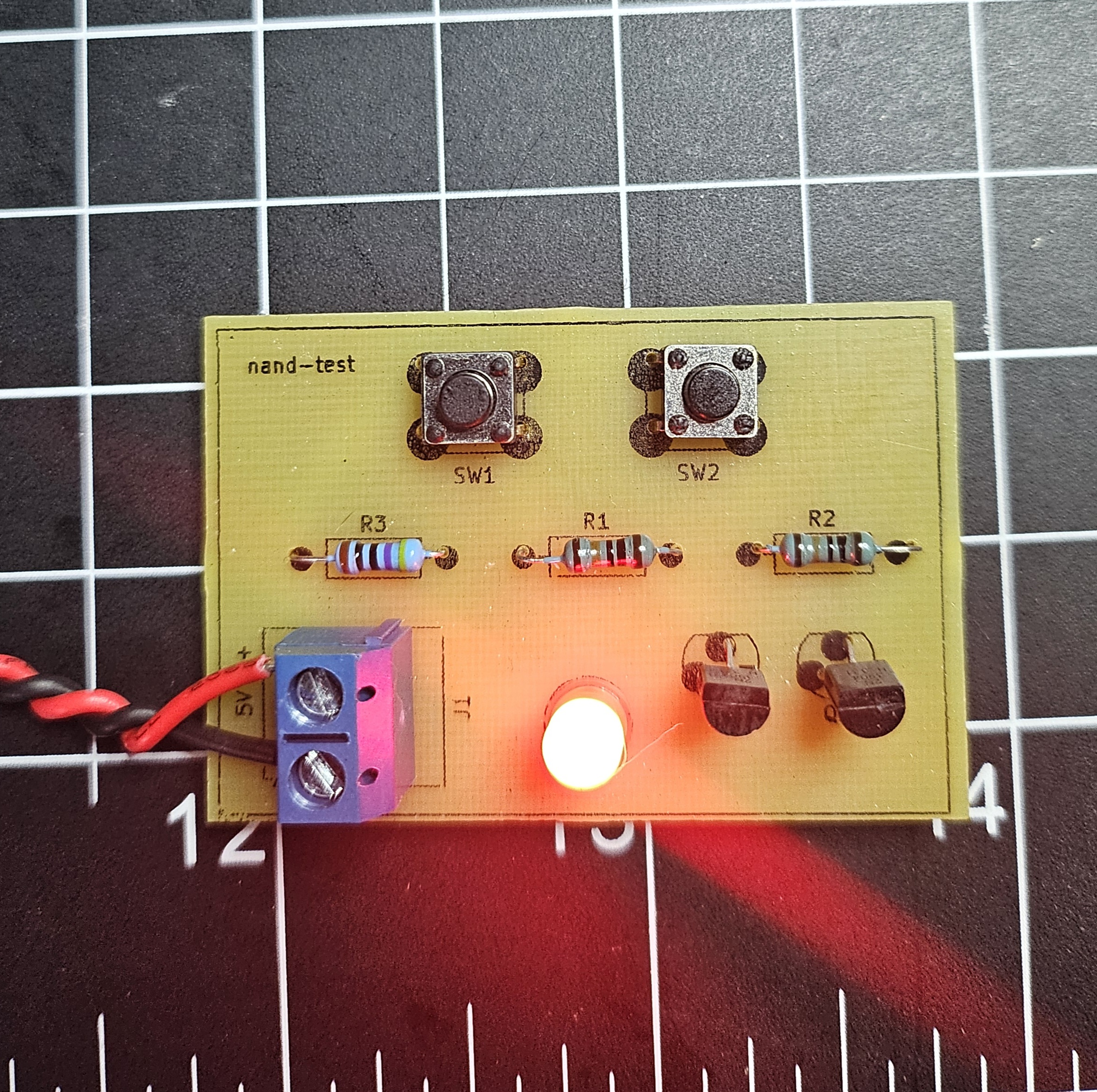
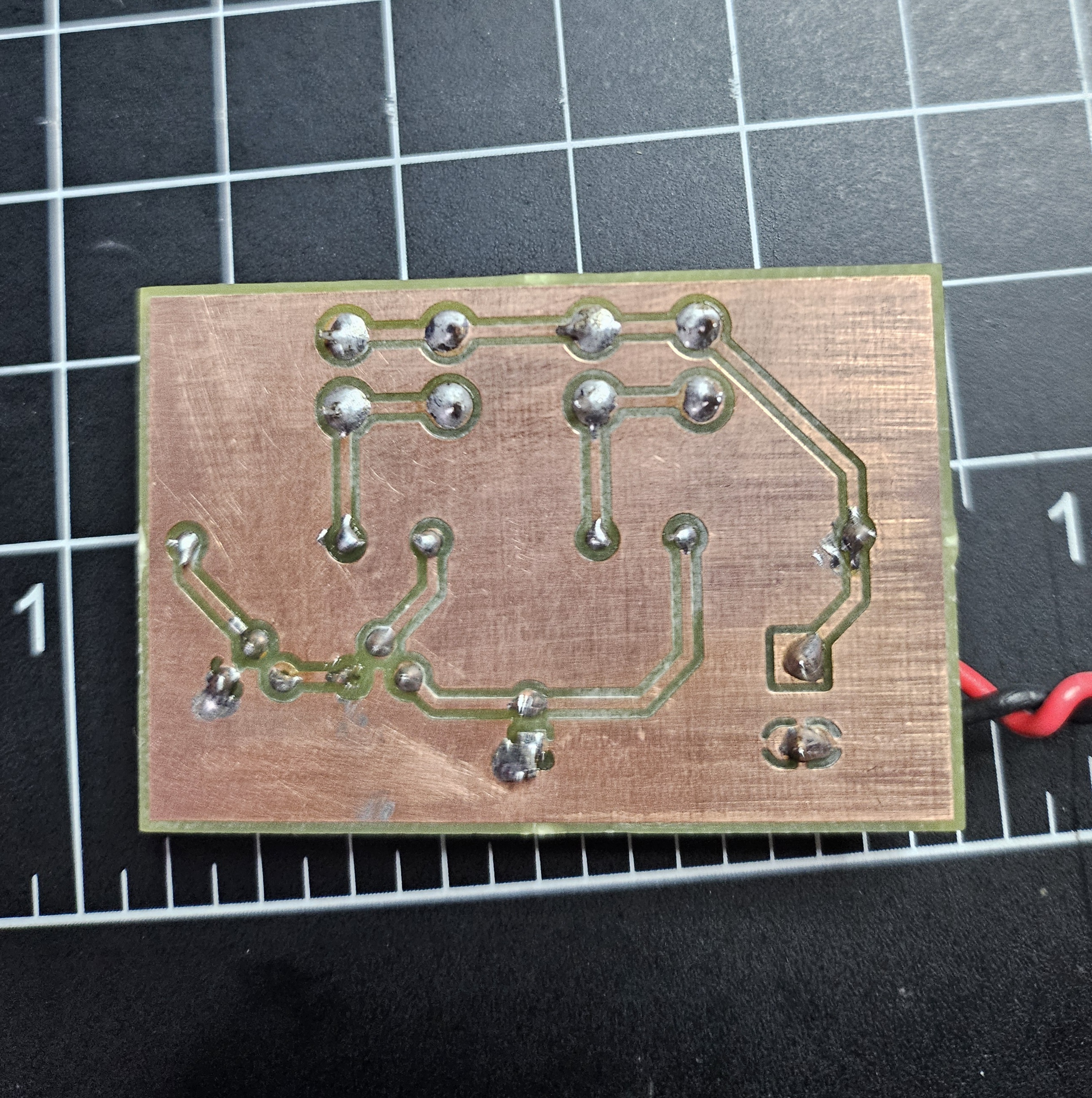
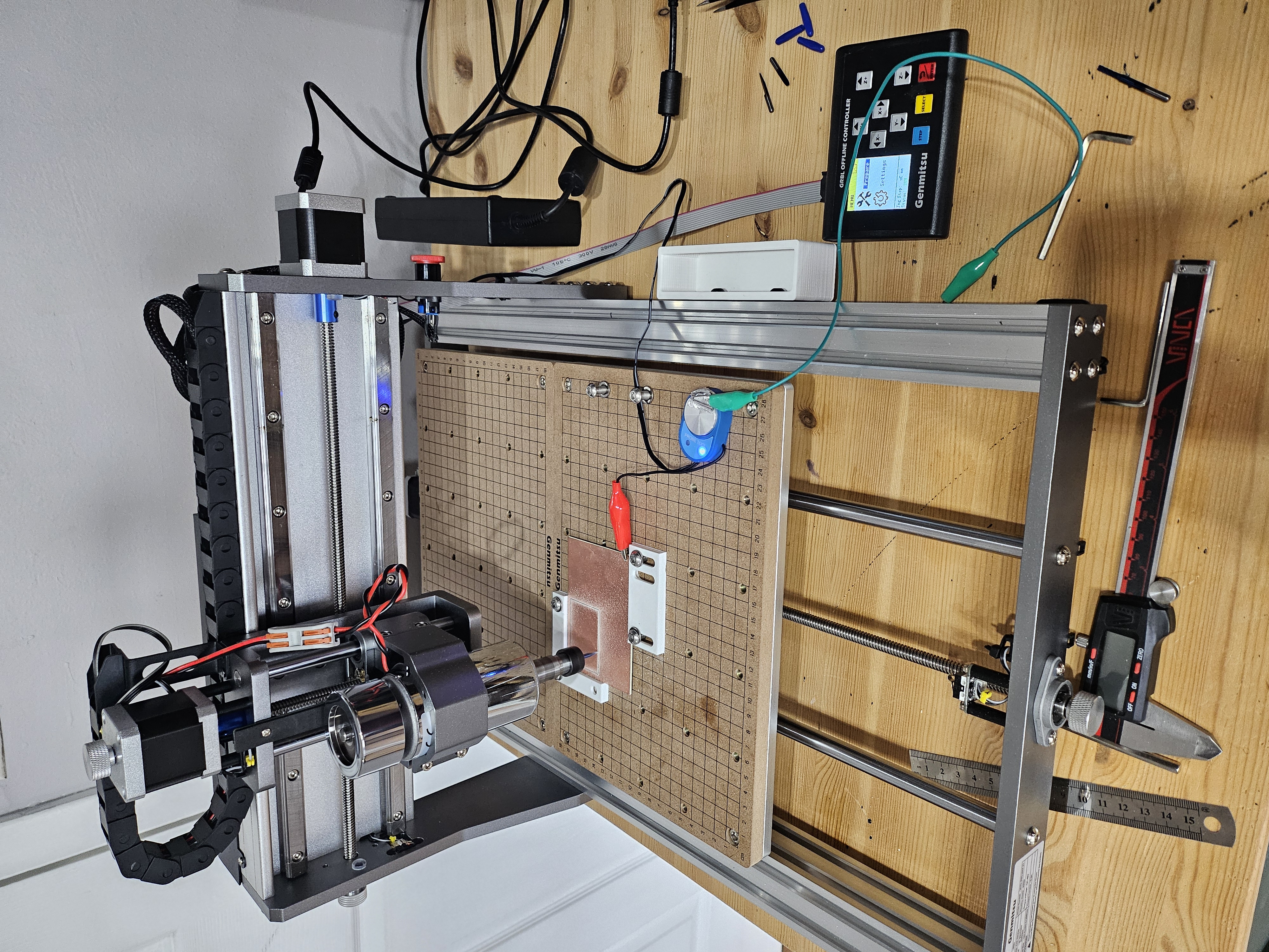
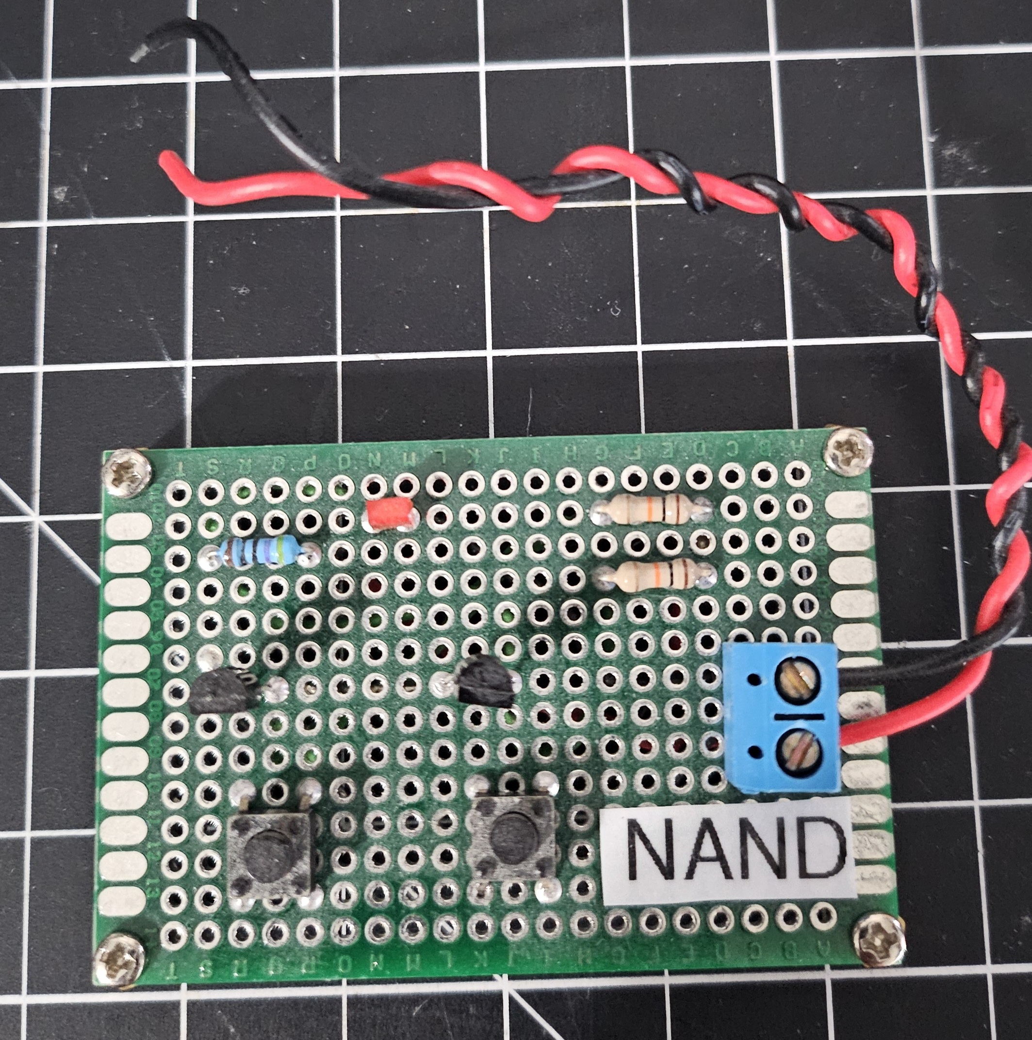
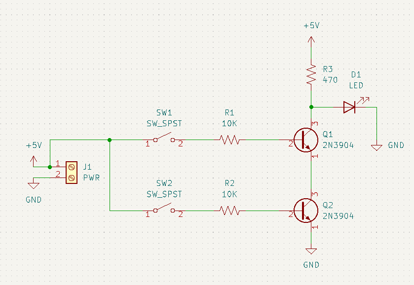
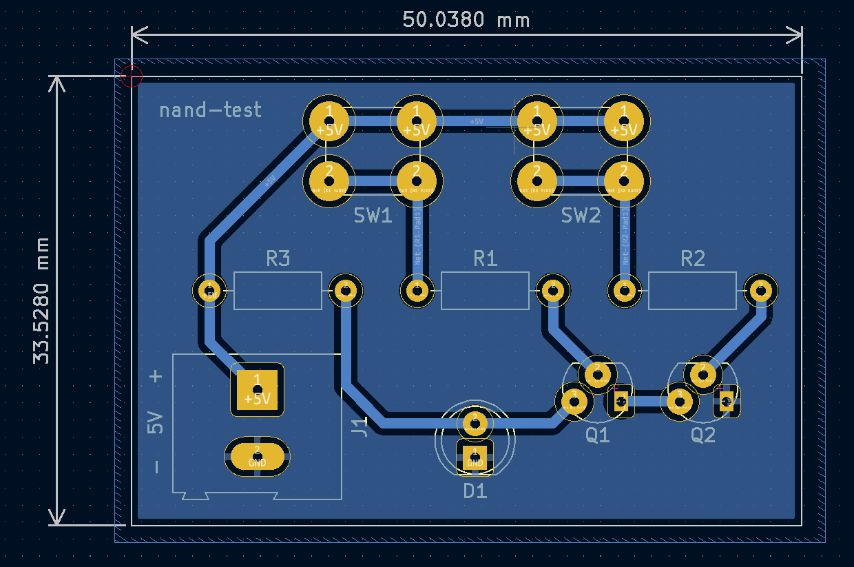
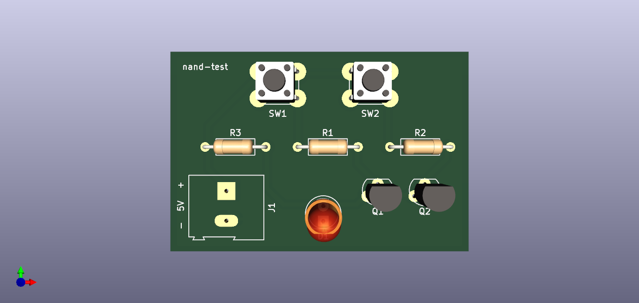
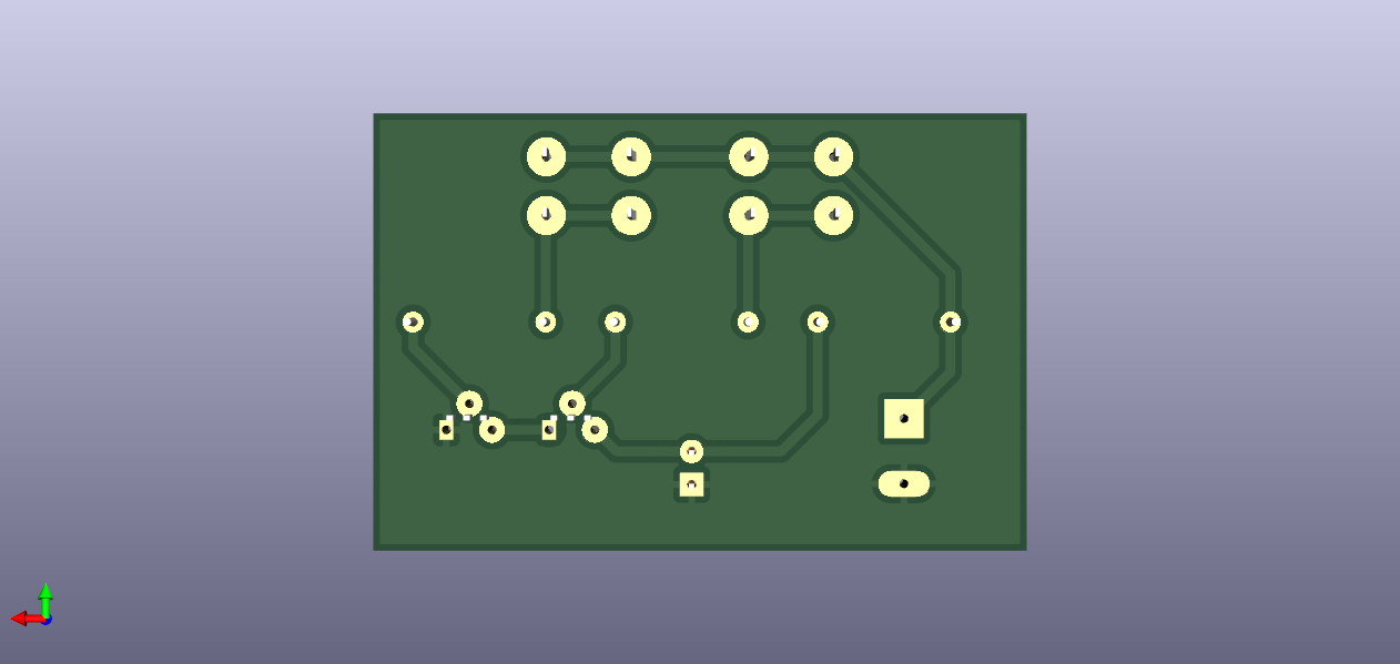
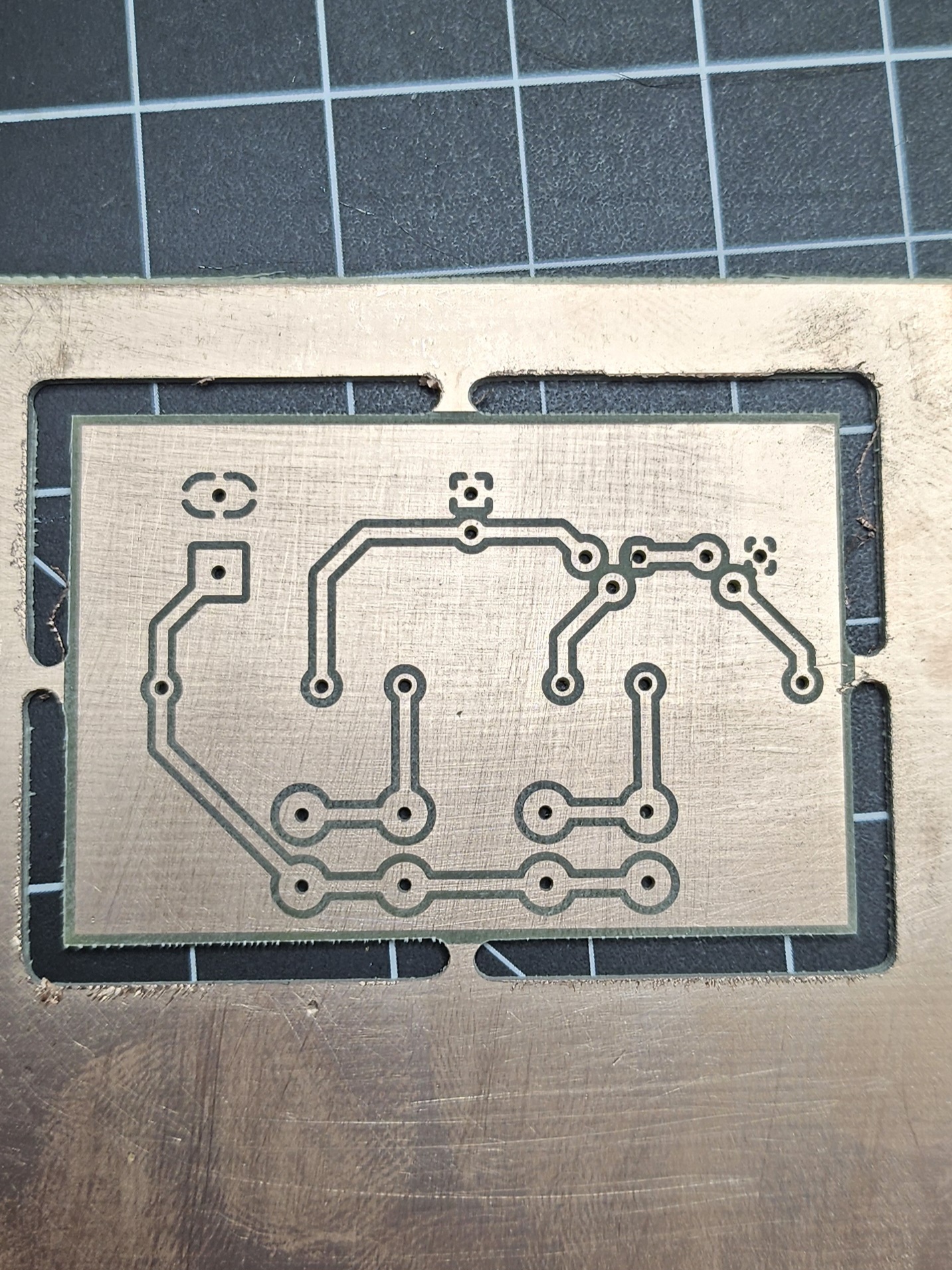
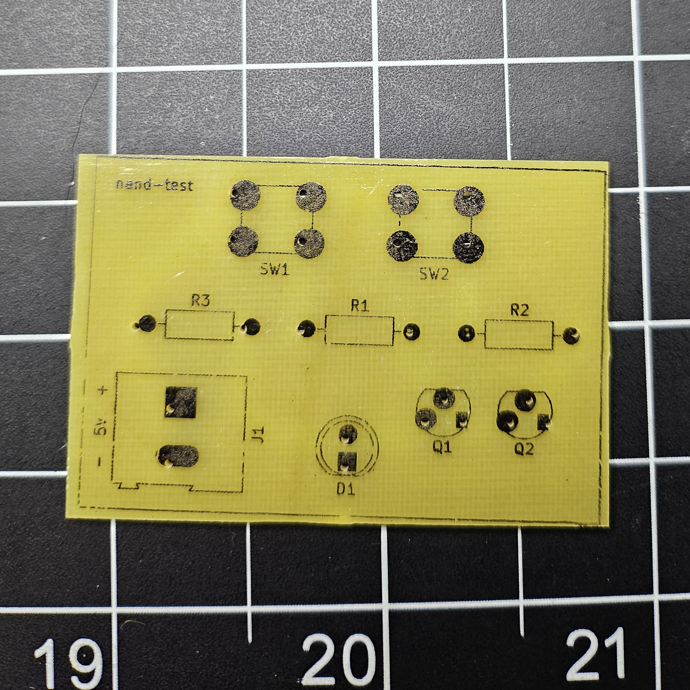
Homemade PCB test using a CNC router.
Hopefully this is useful to someone else wanting a single place to see the whole CNC PCB building process. These notes assume you have a basic understanding of Kicad and Candle (grblcontrol).
There are plenty of companies that offer cheap PCB manufacturing, but I'm impatient and bad at designing things correctly on the first try. Imagine ordering a PCB, waiting a few days, and figuring out you messed up your design. Manufacturing with a CNC router helps to eliminate waiting time between idea and implementation.
Alternatively, plenty of people use the chemical etching process (example: thermal transfer paper and ferric chloride) to build their PCBs. I just don't have a good workspace to mess with nasty chemicals, so the CNC approach is more doable for me. Maybe I'll also add a chemical etching bonus section in the future.
For 2+ sided PCBs, it would be worth ordering from a company. Double-sided PCBs are possible, but I have not attempted this yet. I also haven't tried designs with SMD components yet, so that may also be a pain point that warrants ordering PCBs from a company.
- Genmitsu 3020-PRO MAX V2 CNC Router
- 3040 Y-Axis Extension Kit (optional)
- FR-4 Copper Clad PCB Laminate Board, Single Side, 4 x 2.7 inch (10 piece)
- Bits
- Mini Dry Iron
- Thermal Transfer Paper
- Monochrome Laser Printer
- Mini Drill Press
- Design circuit in Kicad Schematic Editor
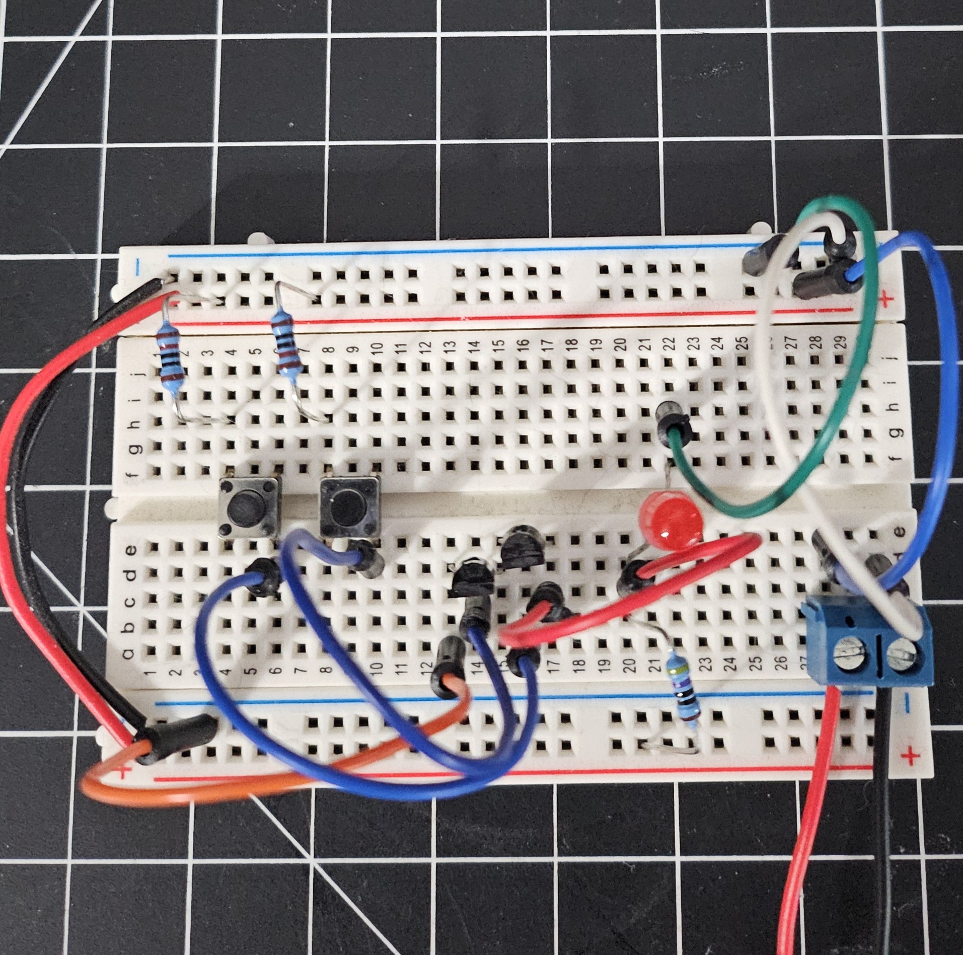
- Breadboard implementation
- Protoboard implementation (optional)
- Kicad Schematic Editor
- Inspect > Electrical Rules Checker
- Tools > Annotate Schematic
- Tools > Assign Footprints
- File > Plot > PDF, Plot All Pages
- Open Kicad PCB Editor (or from Kicad Schematic Editor: Tools > Update PCB From Schematic)
- Generally only use back copper and front silkscreen
- Rearrange rats nest of components to eliminate overlap
- Set design rules (File > Board Setup)
- Minimum clearance: 0.5mm
- Minimum track width: 0.5mm
- Copper to hole clearance: 0.5mm
- Copper to edge clearance: 0.5mm
- Minimum through hole: 0.7mm
- Hole to hole clearance: 0.5mm
- Route tracks on
B.Cu(back copper) layer. Ignore ground pins, will be filled later - Select
Edge.Cutslayer, draw a rectangle to trace board boundary, thickness 1mm - Select
B.Culayer and add fill for ground - Right click fill edge, Zones > Fill Zone
- Add orthogonal dimensions to
User.Drawingslayer to double check board width/height - Place origin at top left of board
- Run Design Rules Checker
- If exporting
F.Silkscreen, I recommend setting text thickness to 0.1mm - Export Gerber files (File > Plot)
- Check Use drill/place file origin
- Export
B.Cu,Edge.Cuts(used in router step) - Export
B.Mask(used in solder masking step) as PDF - Generate Drill Files (
*-NPTH.drland*-PTH.drl)- Drill Origin = Drill/place file origin
- Drill Units = Millimeters
- Print (File > Print)
F.SilkscreenandF.Masklayers to PDF (used in silkscreen step)- Verify Print One Page Per Layer is unchecked
- Scale 1:1
- Select Print Mirrored
Refer to bits listed in Equipment section above.
- Isolation routing: 0.5mm pcb milling bit
- Holes: 0.8mm drill bit
- Edge cut: 2.5mm end mill bit
I know a lot of people seem to recommend v-bits, but I found them to cut too inconsistent to quickly throw together boards.
I did manage to get a couple boards cut with a 0.1mm 60deg bit after manually offsetting my heightmap by 0.05 increments, but I could not replicate this every time. Switching to the pcb milling bit removed ~5-10 minutes of manual adjustment.
- Launch FlatCAM
- Load
B.CuandEdge.Cutsgerber files (File > Open Gerber) - Add drill files (
*.drl) (File > Open Excellon)- Note: Ignore "No geometry found in file" error if no NPTH holes needed
- Options tab
- Set units to mm
- Mirror on y-axis since we're cutting the back copper
- Tool > Double-Sided PCB Tool
- Mirror
B.Cuand*.drlfiles on y-axis using Point/Box
- Select
*-B_Cu.gbr- Isolation Routing section
- Tool dia: 0.45 (note: 0.05 less than clearance set in Kicad)
- Width (# passes): 2
- Pass overlap: 0.10
- Combine Passes: yes
- Click Generate Geometry
- Select
*-B_Cu.gbr_iso- Create CNC Job section
- Cut Z: -0.015
- Travel Z: 2
- Feed Rate: 85.0
- Tool dia: 0.45 (note: 0.05 less than clearance set in Kicad)
- Spindle speed: 10000
- Multi-Depth: yes
- Depth/Pass: 0.08
- Click Generate
- Select
*-B_Cu.gbr_iso_cnc, export G-Code toB_Cu.nc - Select
*-PTH.drl- If too many sizes of drills, go back to Kicad and change hole sizes of individual components (we can always redrill by hand later if holes too small)
- Create CNC Job section
- Cut Z: -2
- Travel Z: 2
- Feed Rate: 100.0
- Tool Change: no (unless using multiple drill sizes)
- Spindle Speed: 10000
- Click Generate
- Select
*-PTH.drl_cnc, set tool dia to 0.8, export G-Code toPTH.drl.nc - Select
*.Edge_Cuts.gbr- Board cutout section
- Tool dia: 2.5
- Margin: 0.1
- Gap size: 1.0
- Gaps: 4
- Click Generate Geometry
- Select
*-Edge_Cuts.gbr_cutout- Create CNC Job section
- Cut Z: -2
- Travel Z: 2.0
- Feed Rate: 50.0
- Tool dia: 2.5
- Spindle speed: 10000
- Multi-Depth: yes
- Depth/pass: 0.25
- Click Generate
- Select
*-Edge_Cuts.gbr_cutout_cnc, export G-Code toEdge_Cuts.nc
- Open
F.SilkscreenPDF in Inkscape (to remove blank space of PDF document)- Select silkscreen components, export
- Export Selection tab, Export Selected Only, 300.0 DPI, SVG
Refer to bits in "Computer Aided Manufacturing (CAM)" section
To secure the PCB to the bed, I used 3D printed M6 Plate Clamps from https://www.printables.com/model/250450-enhancements-for-sainsmartgenmitsu-3020-pro-max-cn/files. Alternatively, I saw a lot of people using carpet tape.
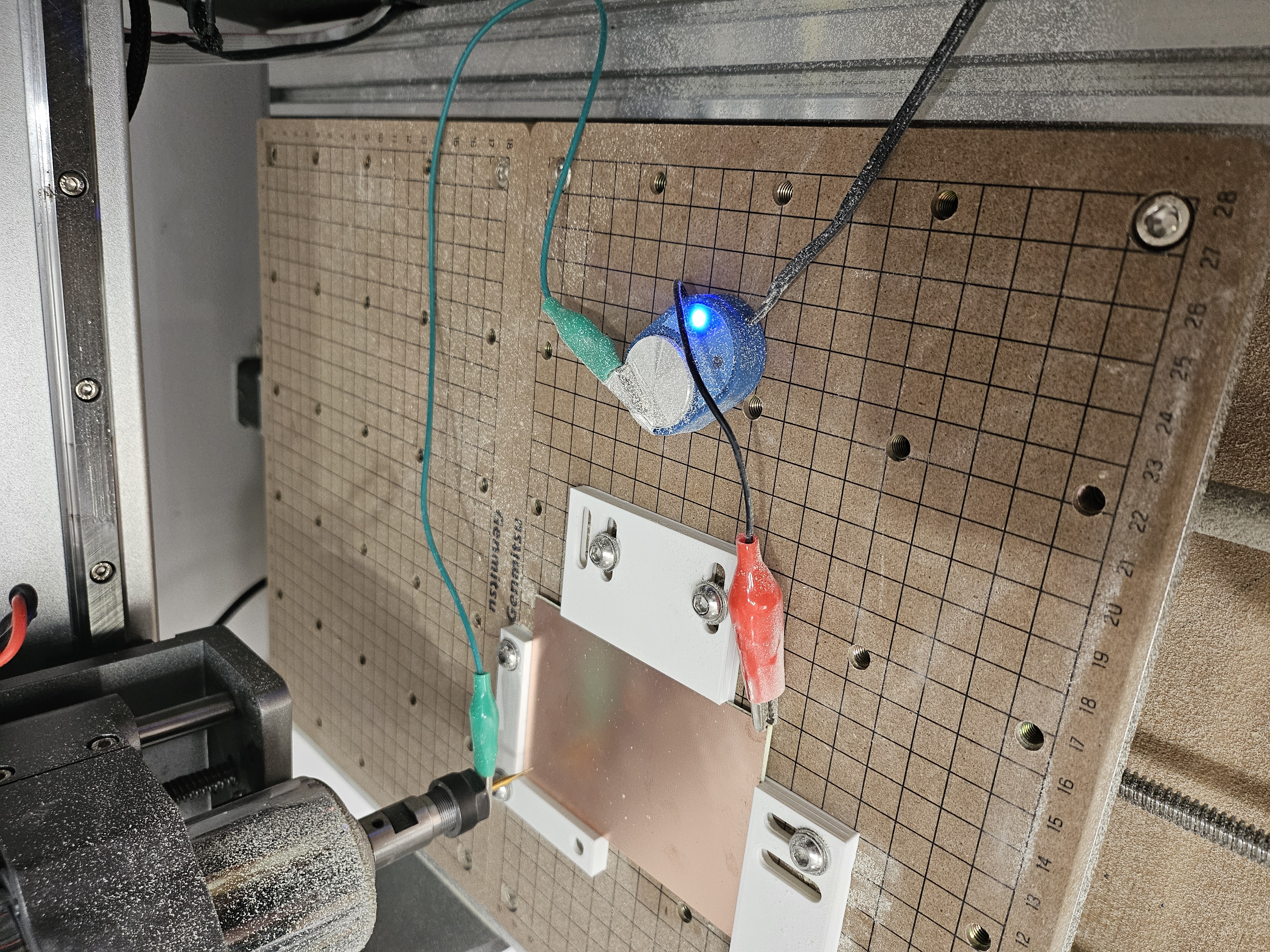
Probe setup using aluminum tape and z-probe that came with CNC router.
- Jog machine to upper left corner, z probe, zero XY
- Height map
- Load nc file, click auto
- Zero XYZ, set bit at origin
- Probe grid, set to be ~10mm apart
- Interpolation grid: 20, 20
- zt = 1.0, zb = -1.0
- Click Probe
- Save as
height.map - Click edit mode to leave edit mode
- Verify use heightmap is checked
- Remove probes
- Load
B.Cu.nc - Swap to drill bit, re-zero Z
- Load
PTH.drl.nc - Swap to edge cut bit, re-zero Z
- Load
Edge_Cuts.nc
- Load thermal transfer paper into printer
- Print
F.SilkscreenSVG onto thermal transfer paper (smooth side up)- Ensure scale is 100%
- Tape thermal paper to front of PCB (toner side down)
- Use highest setting of dry iron to heat evenly for 2-3 minutes
- Apply polycrylic to preserve silkscreen
- Use mini drill press to adjust any holes for larger through hole parts
- Use 400-600 grit sandpaper and/or steel wool to remove any small burrs on back copper
- File down tabs on sides of PCB
- Clean off with a bit of isopropyl alcohol
- Use multimeter to check all tracks for shorts
- Solder components
- Clean off any flux with isopropyl
I tried to do a couple different steps that I hope to try again in the future. I left my notes in archive/.
- Candle
- FlatCAM
- GCODE Reference
- Youtube
- Homemade custom PCB guide using free KiCAD software; Teaching Tech
- Homemade PCB using thermal transfer paper
- Intro to Kicad; Shawn Hymel
- Machining a PCB on the 3-axis CNC Bridgeport Mill; Usagi Electric
- Milling PCBs on a Homemade CNC (Part 2): Masking
- Milling Printed Circuit Boards (PCBs) on a Cheap CNC Machine; Matt's Electronics & RC
- Relay Calculators: Episode 8 - Using FlatCAM and a CNC mill to make PCBs; Usagi Electric
- Sainsmart Genmitsu 3020 Pro Max - 300W Spindle & Linear Rails - Build, Test & Review; techydiy
