A homebrew computer based on the 65C816 processor. Watch the series on YouTube:
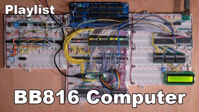
The purpose of this project is to build a 65C816 development platform and learn about the CPU. Conceptually, it will be similar to WDC's own development board.
I'm not going for ludicrous speed and features for revision A, here are the goals:
- Runs at 4Mhz
- Prototyped on a breadboard, through-hole ICs only, no programmable logic
- 32KB RAM, 32KB ROM, 512KB extended RAM
- 65C22 for peripheral I/O
- 65C51 for UART
The goals of the YouTube series are to provide a good description of all the design decisions, including going in-depth on timing, to be a more advanced complement to something like Ben Eater's 6502 series, as well as show more love to this cool CPU in the homebrew community.


- BusBoard BB830 Breadboards
- Hook-Up Wire: Recommended option
- Male-to-Male Dupont Wires
- Dupont Female Connectors. Use them to replace single connectors and group your cables by 2, 8...
- 10uF Polarized capacitors. Sprinkle one per power rail
- 3mm LEDs with built-in resistors (Yellow, Red, Green)
- LED Bars with 8 LEDs, various colors (Red version), with 9-pin bussed 1k resistors. I use 1k, 1.5k or 3.3k resistors depending on the color.
- ZIF socket for ROM: Aries Electronics 28-526-10 + 28pin Wire-Wrap socket
Component Count: 81
| Refs | Qty | Component | Description |
|---|---|---|---|
| C1 | 1 | 220u | Polarized capacitor, small symbol |
| C2, C4, C5, C6, C7, C8, C9, C10, C11, C12, C13, C14, C15, C16, C17, C18, C19 | 17 | 100n | Unpolarized capacitor, small symbol |
| C3 | 1 | 10u | Polarized capacitor, small symbol |
| D1 | 1 | POWER | Light emitting diode, small symbol |
| D2 | 1 | 1N5817 | 20V 1A Schottky Barrier Rectifier Diode, DO-41 |
| J1 | 1 | Barrel_Jack_Switch | DC Barrel Jack with an internal switch |
| J2 | 1 | Conn_02x40_Odd_Even | Generic connector, double row, 02x40, odd/even pin numbering scheme (row 1 odd numbers, row 2 even numbers), script generated (kicad-library-utils/schlib/autogen/connector/) |
| J3 | 1 | Conn_02x18_Odd_Even | Generic connector, double row, 02x18, odd/even pin numbering scheme (row 1 odd numbers, row 2 even numbers), script generated (kicad-library-utils/schlib/autogen/connector/) |
| R1, R2, R3, R5, R11, R17 | 6 | 3.3k | Resistor, small symbol |
| R4, R12, R13, R14, R15 | 5 | 100k | Resistor, small symbol |
| R6, R16 | 2 | 1k | Resistor, small symbol |
| R7, R8, R9, R10 | 4 | 0R | Resistor, small symbol |
| RN1 | 1 | 100k | 8 resistor network, star topology, bussed resistors, small symbol |
| RN2, RN3, RN4 | 3 | 100k | 8 resistor network, star topology, bussed resistors, small symbol |
| RN5 | 1 | 100k | 8 resistor network, star topology, bussed resistors, small symbol |
| SW1 | 1 | RESET | Push button switch, generic, two pins |
| U1 | 1 | 74AHC74 | Dual D Flip-flop, Set & Reset |
| U2 | 1 | 74AHC00 | quad 2-input NAND gate |
| U3 | 1 | 74AC112 | dual JK Flip-Flop, Set & Reset |
| U4 | 1 | W65C816SxP | W65C816S 8/16-bit CMOS General Purpose Microprocessor, DIP-40 |
| U5, U6, U12 | 3 | 74AHC32 | Quad 2-input OR |
| U7 | 1 | 74AHC125 | Quad buffer 3-State outputs |
| U8 | 1 | DS1813-5 | |
| U9, U14 | 2 | 74HC74 | Dual D Flip-flop, Set & Reset |
| U10 | 1 | 74AHCT245 | Octal BUS Transceivers, 3-State outputs |
| U11 | 1 | 74AHC573 | 8-bit Latch 3-state outputs |
| U13 | 1 | 74AHC02 | quad 2-input NOR gate |
| U15 | 1 | 74AC10 | Triple 3-input NAND |
| U16 | 1 | DS1035-10 | 3-in-1 High–Speed Silicon Delay Line |
| X1 | 1 | 8MHz | Crystal Clock Oscillator, DIP8-style metal package |
Component Count: 167
| Refs | Qty | Component | Description |
|---|---|---|---|
| BAR1 | 1 | LED-Array-10-BGYR | BAR GRAPH 10 segment |
| BAR2, BAR3, BAR4 | 3 | Yellow | BAR GRAPH 8 segment |
| BAR5 | 1 | Green | BAR GRAPH 8 segment |
| BAR6, BAR7, BAR8 | 3 | Red | BAR GRAPH 8 segment |
| BAR9, BAR10 | 2 | LED-Array-8-GYR | BAR GRAPH 10 segment |
| C1, C6, C10, C27 | 4 | 10u | Polarized capacitor, small symbol |
| C2, C3, C4, C5, C7, C8, C9, C12, C16, C17, C18, C19, C20, C21, C22, C23, C24, C28, C29, C30, C31, C32, C33, C34, C35, C36, C37, C38, C39, C41, C42, C43, C44 | 33 | 100n | Unpolarized capacitor, small symbol |
| C11 | 1 | 22u | Polarized capacitor, small symbol |
| C13, C14, C15 | 3 | 2.2u | Polarized capacitor, small symbol |
| C25 | 1 | 1u | Polarized capacitor, small symbol |
| C26 | 1 | 10n | Unpolarized capacitor, small symbol |
| C40 | 1 | 470n | Unpolarized capacitor, small symbol |
| D1 | 1 | Clock | Light emitting diode, small symbol |
| D2, D7 | 2 | 1N5819 | 40V 1A Schottky Barrier Rectifier Diode, DO-41 |
| D8 | 1 | Slow | Light emitting diode, small symbol |
| D9 | 1 | Fast | Light emitting diode, small symbol |
| D10 | 1 | Pulse | Light emitting diode, small symbol |
| DS1 | 1 | HD44780 | LCD 16x2 Alphanumeric , 8 bit parallel bus, 5V VDD |
| J1 | 1 | Tester | Generic connector, single row, 01x08, script generated (kicad-library-utils/schlib/autogen/connector/) |
| J2 | 1 | USB_B | USB Type B connector |
| J3 | 1 | USB_I2C | Generic connector, single row, 01x04, script generated (kicad-library-utils/schlib/autogen/connector/) |
| J4 | 1 | USB Reset | Generic connector, single row, 01x02, script generated (kicad-library-utils/schlib/autogen/connector/) |
| R1, R9, R10, R11, R12, R13, R14, R15, R19, R20, R34, R35, R36 | 13 | 3.3k | Resistor, small symbol |
| R2, R4, R6, R8 | 4 | 10k | Resistor, small symbol |
| R3, R5, R7 | 3 | 2.2k | Resistor, small symbol |
| R16, R18, R25, R26, R27, R31, R32, R37, R38, R39, R41, R42 | 12 | 1k | Resistor, small symbol |
| R17 | 1 | 220 | Resistor, small symbol |
| R21, R22, R23, R24, R33, R43, R44, R45, R46, R47, R48, R49, R50, R51 | 14 | 6.8k | Resistor, small symbol |
| R28, R29, R30, R40 | 4 | 1.5k | Resistor, small symbol |
| RN1, RN2, RN3 | 3 | 1k | 8 resistor network, star topology, bussed resistors, small symbol |
| RN4, RN7 | 2 | 3.3k | 8 resistor network, star topology, bussed resistors, small symbol |
| RN5, RN6, RN8 | 3 | 1.5k | 8 resistor network, star topology, bussed resistors, small symbol |
| RV1 | 1 | 500k | Potentiometer |
| RV2 | 1 | 10k | Potentiometer |
| SW1 | 1 | Pulse | Push button switch, generic, two pins |
| SW2 | 1 | Mode | Push button switch, generic, two pins |
| SW3 | 1 | Speed | Push button switch, generic, two pins |
| SW4 | 1 | SW_DIP_SPDT_x02 | 2x DIP Switch, Single Pole Double Throw (SPDT) switch, small symbol |
| SW5 | 1 | SW_DIP_x03 | 3x DIP Switch, Single Pole Single Throw (SPST) switch, small symbol |
| SW6 | 1 | SW_DIP_x08 | 8x DIP Switch, Single Pole Single Throw (SPST) switch, small symbol |
| U1 | 1 | 65C816-Breakout | See https://github.com/adrienkohlbecker/BB816/tree/main/hardware/breakout |
| U2 | 1 | 74HC30 | 8-input NAND |
| U3 | 1 | 74AHC00 | quad 2-input NAND gate |
| U4 | 1 | 74AHC32 | Quad 2-input OR |
| U5 | 1 | 74AHC138 | Decoder 3 to 8 active low outputs |
| U6 | 1 | AT28C256-15PC | Paged Parallel EEPROM 256Kb (32K x 8), DIP-28/SOIC-28 |
| U7 | 1 | LY62256PL-55LL | 32Kx8 bit Low Power CMOS Static RAM, 55/70ns, DIP-28 |
| U8 | 1 | AS6C4008-55PCN | 512K x 8 Low Power CMOS RAM, DIP-32 |
| U9 | 1 | 74HC14 | Hex inverter schmitt trigger |
| U10, U12, U14 | 3 | 74HC74 | Dual D Flip-flop, Set & Reset |
| U11 | 1 | 74HC32 | Quad 2-input OR |
| U13 | 1 | 74HCT193 | Synchronous 4-bit Up/Down (2 clk) counter |
| U15, U31 | 2 | 74AHC74 | Dual D Flip-flop, Set & Reset |
| U16 | 1 | LMC555xN | CMOS Timer, 555 compatible, PDIP-8 |
| U17 | 1 | 74HC251 | Multiplexer 8 to 1, 3-state Outputs |
| U18 | 1 | 74HC153 | Dual Multiplexer 4 to 1 |
| U19 | 1 | 74HC04 | Hex Inverter |
| U20 | 1 | 74HC540 | 8-bit Buffer/Line driver Inverter, 3-state outputs |
| U21, U22, U23, U24, U27, U28, U32, U33 | 8 | 74HC541 | 8-bit Buffer/Line Driver 3-state outputs |
| U25 | 1 | Teensy++2.0 | |
| U26 | 1 | W65C22SxP | W65C22S CMOS Versatile Interface Adapter (VIA), 20-pin I/O, 2 Timer/Counters, DIP-40 |
| U29 | 1 | W65C51NxP | W65C51N CMOS Asynchronous Communication Interface Adapter (ACIA), Serial UART, DIP-28 |
| U30 | 1 | MCP2221AxP | USB to I2C/UART Protocol Converter with GPIO, DIP-14 |
| X1 | 1 | 8MHz | Crystal Clock Oscillator, DIP14-style metal package |
| X2 | 1 | 1.8432MHz | Crystal Clock Oscillator, DIP8-style metal package |
TODO: This hasn't been updated in a while
| Refs | Qty | Component | Description |
|---|---|---|---|
| U* | 1 | 74AC08 | Quad And2 |
DS1035-10: can be replaced byDS1135Z-10+with a SOIC-8 to through hole adapterTeensy++ 2.0: While it is not manufactured by PJRC anymore, clones of this board are available on sites such as Aliexpress


View source
Uses custom fork
{
  signal: [
    { name: 'CLK_SRC', wave: '0..(25)x(10)1(40)x(10)0(17)', phase: 0.20 },
    { nodes: ['...(25)Ο(5)Ό(5)G(40)H(5)R(5)P', '...(30)Ν(10)Ά(40)Β(10)Ξ'], phase: 0.45 },
    { name: 'CLK-', wave: '0..(37.5)x(5)1(45)x(5)0..(7.5)', phase: 0.20 },
    { nodes: ['...(37.5)Ё(2.5)Ж(2.5)S(45)T(2.5)Ћ(2.5)Δ', '...(40)L(10)K(40)M(10)Σ'], phase: 0.45 },
    { name: 'CLK', wave: '1.0(50)1(50)0.', phase: 0.20 },
    { nodes: ['..Θ(10)Λ(40)Њ(10)Ќ', '...(7.5)Љ(2.5)Є(2.5)Υ(45)Ю(2.5)Ψ(2.5)Ω'], phase: 0.45 },
    { name: 'CLK+', wave: '1..(7.5)x(5)0(45)x(5)1..(37.5)', phase: 0.20 },
    {},
    { nodes: ['..Ε(8.5)Ι(41.5)Κ(8.5)Μ', '..Ρ(1)Τ(49)Χ(1)А'], phase: 0.45 },
    { name: '~CLK', wave: '0..(1)x(7.5)1(42.5)x(7.5)0..(41.5)', phase: 0.20 },
  ],
  edge: [
    'Ν+Ά 10ns', 'Β+Ξ 10ns', 'Ο+Ό 5ns', 'Ό+G 5ns', 'H+R 5ns', 'R+P 5ns',
    'L+K 10ns', 'M+Σ 10ns', 'Ё+Ж 2.5ns', 'Ж+S 2.5ns', 'T+Ћ 2.5ns', 'Ћ+Δ 2.5ns',
    'Θ+Λ 10ns', 'Њ+Ќ 10ns', 'Љ+Є 2.5ns', 'Є+Υ 2.5ns', 'Ю+Ψ 2.5ns', 'Ψ+Ω 2.5ns',
    'Ε+Ι 8.5ns', 'Κ+Μ 8.5ns', 'Ρ+Τ 1ns', 'Χ+А 1ns'
  ],
  config: {
    skin: 'narrower',
    lines: {
      offset: 2,
      every: 50
    },
    background: 'white',
  },
  head: {
    tick: -2,
    every: 10,
    text: ['tspan', { "font-size": '12px' }, 'based on 10Mhz clock']
  }
}
View source
Uses custom fork
{
  signal: [
    { name: 'CLK', wave: '1.0(125)1(125)0.', phase: 0.20 },
    { nodes: ['..Ѳ(10)Ѵ(115)Ά(10)Β', '...(7.5)Α(2.5)Γ(2.5)Ν(120)Ξ(2.5)Ο(2.5)Ό'], phase: 0.90 },
    { name: 'CLK+', wave: '1..(7.5)x(5)0(120)x(5)1..(112.5)', phase: 0.20 },
    { nodes: ['..B(33)Π', '..A(10)D(115)E(10)F(105)G(10)H'], phase: 0.90 },
    { name: 'CPU D0-D7 (read)', wave: '6..(10)x(23)7(102)x(105)6..(10)', data: ['Rd Data', 'Bank Address', 'Rd Data'], phase: 0.20 },
    { nodes: ['..K(33)C(92)Σ(30)I', '..Ρ(10)L(23)C(92)M(10)N'], phase: 0.90 },
    { name: 'CPU D0-D7 (write)', wave: '6(12)x(23)7(102)x(20)6(97)', data: ['Wr Data', 'Bank Address', 'Write Data'], phase: 0.20 },
    { nodes: ['...(12.5)Я(17)P(95.5)Τ(8.5)S', '...(7.5)J(2)O..(113.5)Q(1)R'], phase: 0.90 },
    { name: '/READ_CLOCK', wave: '0..(9.5)x(20)1(96.5)x(7.5)0(118.5)', node: '..(123.5)É(3.5)È.(6.5)À(1.5)Ç', phase: 0.20, nphase: 0.90, nyoffset: -6 },
    { nodes: ['..(34)Υ(11)Z'], phase: 0.90 },
    { nodes: ['...(33)X(1)Y', '...(9.5)T(1)U(19)V(12)W'], phase: 0.90 },
    { name: 'BA0-BA7', wave: '7..(10.5)x(33.5)7(208)', data: ['BA', 'Bank Address'], phase: 0.20 },
  ],
  edge: [
    'Ѳ+Ѵ 10ns', 'Α+Γ 2.5ns', 'Γ+Ν 2.5ns', 'Ά+Β 10ns', 'Ξ+Ο 2.5ns', 'Ο+Ό 2.5ns',
    'A+D 10ns', 'B+Π 33ns', 'E+F 10ns', 'G+H 10ns',
    'Ρ+L 10ns', 'K+C 33ns', 'M+N 10ns', 'Σ+I 30ns',
    'J+O 2ns', 'Я+P 17ns', 'Q+R 1ns', 'Τ+S 8.5ns',
    'T+U 1ns', 'V+W 12ns', 'X+Y 1ns', 'Υ+Z 11s',
    'É+È 3.5ns', 'À+Ç 1.5ns',
  ],
  config: {
    skin: 'narrowerer',
    lines: {
      offset: 2,
      every: 125
    },
    background: 'white'
  },
  head: {
    tick: -2,
    every: 10,
    text: ['tspan', { "font-size": '12px' }, 'based on 4Mhz clock; assumes BE=RDY=1']
  }
}
View source
Uses custom fork
{
  signal: [
    { name: 'CLK', wave: '1.0(125)1(125)0.', phase: 0.20 },
    { nodes: ['..Ѳ(10)Ѵ(115)Ά(10)Β', '...(7.5)Α(2.5)Γ(2.5)Ν(120)Ξ(2.5)Ο(2.5)Ό'], phase: 0.9 },
    { name: 'CLK+', wave: '1..(7.5)x(5)0(120)x(5)1..(112.5)', phase: 0.20 },
    { nodes: ['..B(33)Π', '..A(10)D(115)E(10)F(105)G(10)H'], phase: 0.9 },
    { name: 'CPU D0-D7 (read)', wave: '6..(10)x(23)7(102)x(105)6..(10)', data: ['Rd Data', 'Bank Address', 'Rd Data'], phase: 0.20 },
    { nodes: ['..K(33)C(92)Σ(30)I', '..Ρ(10)L(23)C(92)M(10)N'], phase: 0.9 },
    { name: 'CPU D0-D7 (write)', wave: '6(12)x(23)7(102)x(20)6(97)', data: ['Wr Data', 'Bank Address', 'Write Data'], phase: 0.20 },
    { nodes: ['..Ύ(30)Д', '..Б(10)Г'], phase: 0.9 },
    { name: 'AHCT245 DIR', wave: '3..(10)x(20)3(220)..', data: ['RWB', 'RWB'], phase: 0.20 },
    { node: '...(10)Ё(1)Ж(19)З(17.5)И', phase: 0.9 },
    { name: 'AHCT245 OUT', wave: '2..(11)x(36.5)2(202.5)..', data: ['DIR valid', 'DIR valid'], phase: 0.20 },
    { nodes: ['...(11)(2.5)І(16.5)Л(97)(11)(2.5)Ѣ(15)Ц', '...(7.5)Й(2)К(116.5)(7.5)П(2)Ф'], phase: 0.9 },
    { name: 'AHCT245 OE', wave: '0..(9.5)x(19.5)1(105.5)x(18)0(97.5)..', data: ['RWB', 'RWB'], phase: 0.20 },
    { node: '...(9.5)Ч(1)Ш(18.5)Щ(17.5)Ъ(88)Ы(1)Ь(17)Э(17)Ю', phase: 0.9 },
    { name: 'AHCT245 OUT', wave: '2..(10.5)x(36)2(89)x(34)2(80.5)..', data: ['ON', 'OFF', 'ON'], phase: 0.20 },
    { nodes: ['..Ε(10)Δ', '..(10)Φ(1)Έ(219)Ζ(11)Η(10)Ή'], phase: 0.9 },
    { name: 'AHCT245 OUT (read)', wave: '2..(9)x(220)2(21)..', data: ['Rd Data', 'Read Data'], phase: 0.20 },
    { node: '..Θ(10)Ι(1)Ί(114)Κ(30)Λ(11)Μ', phase: 0.9 },
    { name: 'AHCT245 OUT (write)', wave: '2..(11)x(155)2(84)..', data: ['Wr Data', 'Write Data'], phase: 0.20 },
    { nodes: ['..Z(9)R(220)P(21)J'], phase: 0.9 },
    { name: 'D0-D7 (read)', wave: '6..(9)x(220)6(21)..', data: ['Rd Data', 'Read Data'], phase: 0.20 },
    { node: '..T(10.5)Y(114.5)U(44.5)O', phase: 0.9 },
    { name: 'D0-D7 (write)', wave: '6..(10.5)x(159)6(80.5)..', data: ['Wr Data', 'Write Data'], phase: 0.20 },
  ],
  edge: [
    'Ѳ+Ѵ 10ns', 'Α+Γ 2.5ns', 'Γ+Ν 2.5ns', 'Ά+Β 10ns', 'Ξ+Ο 2.5ns', 'Ο+Ό 2.5ns',
    'A+D 10ns', 'B+Π 33ns', 'E+F 10ns', 'G+H 10ns',
    'Ρ+L 10ns', 'K+C 33ns', 'M+N 10ns', 'Σ+I 30ns',
    'Б+Г 10ns', 'Ύ+Д 30ns',
    'Ё+Ж 1ns', 'З+И 17.5ns',
    'Й+К 2ns', 'І+Л 16.5ns', 'П+Ф 2ns', 'Ѣ+Ц 15ns',
    'Ч+Ш 1ns', 'Щ+Ъ 17.5ns', 'Ы+Ь 1ns', 'Э+Ю 17ns',
    'Ε+Δ 10ns', 'Φ+Έ 1ns', 'Ζ+Η 11ns', 'Η+Ή 10ns',
    'Θ+Ι 10ns', 'Ι+Ί 1ns', 'Κ+Λ 30ns', 'Λ+Μ 11ns',
    'Z+R 9ns', 'P+J 21ns', 'T+Y 10.5ns', 'U+O 44.5ns'
  ],
  config: {
    skin: 'narrowerer',
    lines: {
      offset: 2,
      every: 125
    },
    background: 'white'
  },
  head: {
    tick: -2,
    every: 10,
    text: ['tspan', { "font-size": '12px' }, 'based on 4Mhz clock; assumes BE=RDY=1']
  }
}
View source
Uses custom fork
{
  signal: [
    { name: 'CLK', wave: '1.0(100)1.', phase: 0.20 },
    { nodes: ['..Ѳ(30)Ѵ', '..Α(10)Γ'], phase: 0.45 },
    { name: 'A[0..15]', wave: '3..(10)x(20)3(70)..', data: ['', 'Address'], phase: 0.20 },
    { nodes: ['..Β(44)Ξ', '..Ν(10.5)Ά'], phase: 0.45 },
    { name: 'A[16..23]', wave: '7..(10.5)x(33.5)7(58)', data: ['', 'Bank Address'], phase: 0.20 },
    { nodes: ['..Ο(69.5)Ό', '..A(11.5)D'], phase: 0.45 },
    { name: 'EXTRAM_CS', wave: '8..(11.5)x(58)8(32.5)', data: ['', 'Extended RAM'], phase: 0.20 },
    { nodes: ['..B(78)Π', '..E(12)F'], phase: 0.45 },
    { name: 'ROM_CS', wave: '8..(12)x(66)8(24)', data: ['', 'ROM'], phase: 0.20 },
    { nodes: ['..G(81)H', '..Ρ(11)L'], phase: 0.45 },
    { name: 'IO_CS', wave: '8..(11)x(70)8(21)', data: ['', 'I/O'], phase: 0.20 },
    { nodes: ['..K(78)C', '..M(12)N'], phase: 0.45 },
    { name: 'RAM_CS', wave: '8..(12)x(66)8(24)', data: ['', 'RAM'], phase: 0.20 },
  ],
  edge: [
    'Ѳ+Ѵ 30ns', 'Α+Γ 10ns', 'Ν+Ά 10.5ns', 'Β+Ξ 44ns', 'Ο+Ό 69.5ns',
    'A+D 11.5ns', 'B+Π 78ns', 'E+F 12ns', 'G+H 81ns',
    'Ρ+L 11ns', 'K+C 78ns', 'M+N 12ns',
  ],
  config: {
    skin: 'narrower',
    lines: {
      offset: 2,
      every: 100
    },
    background: 'white'
  },
  head: {
    tick: -2,
    every: 10,
    text: ['tspan', { "font-size": '12px' }, 'based on 5Mhz clock; assumes BE=RDY=1']
  }
}
View source
Uses custom fork
{
  signal: [
    { name: 'BE', wave: '1....0(40)1(40)0(2)', phase: 0.20 },
    { nodes: ['.....Ѳ(25)Ѵ(15)Ρ(25)L'], phase: 0.45 },
    { name: 'CPU ADDR & RWB', wave: '7....x(25)9(15)x(25)7(15)x(2)', data:['ON', 'OFF', 'ON'], phase: 0.20 },
    { nodes: ['.....Ά(8.5)Ν(31.5)M(8.5)N', '.....Α(1)Γ(39)K(1)C'], phase: 0.45 },
    { name: '!BE', wave: '0.....(1)x(7.5)1(32.5)x(7.5)0(32.5)x(1)', phase: 0.20 },
    { nodes: ['......(8.5)Β(12)Ξ(28)J(12)O', '......(1)Ο(1)Ό(39)Σ(1)I'], phase: 0.45 },
    { name: 'AHC573 OUT', wave: '7.....(2)x(18.5)9(21.5)x(18.5)7(21.5)', data:['ON', 'OFF', 'ON'], phase: 0.20 },
    { nodes: ['.....A(8)D(32)Q(6.5)R', '.....B(1)Π(39)Я(1)P'], phase: 0.45 },
    { name: 'AHCT245 OE', wave: '0.....(1)x(7)1(33)x(5.5)0(34.5)x(1)', phase: 0.20 },
    { nodes: ['......(8.5)E(17.5)F(20.5)T(17)U', '......(1)G(1)H(39)Τ(1.5)S'], phase: 0.45 },
    { name: 'AHCT245 OUT', wave: '7.....(2)x(24)9(16.5)x(21)7(18.5)', data:['ON', 'OFF', 'ON'], phase: 0.20 },
    { nodes: ['......(8.5)V(10)W(30)Б(8)Г', '......(1)X(1)Y(39)Ύ(1)Д'], phase: 0.45 },
    { name: 'RD & WR', wave: '7.....(2)x(16.5)9(23.5)x(14.5)7(25.5)', data:['ON', 'OFF', 'ON'], phase: 0.20 },
  ],
  edge: [
    'Ѳ+Ѵ 25ns', 'Α+Γ 1ns', 'Ά+Ν 8.5ns', 'Ο+Ό 1ns', 'Ξ+Β 12ns',
    'B+Π 1ns', 'A+D 8ns', 'G+H 1ns','E+F 17.5ns',
    'Ρ+L 25ns', 'K+C 1ns', 'M+N 8.5ns', 'Σ+I 1ns', 'J+O 12ns',
    'Я+P 1ns', 'Q+R 6.5ns', 'Τ+S 1ns','T+U 17ns',
    'V+W 10ns', 'X+Y 1ns', 'Б+Г 8ns', 'Ύ+Д 1ns',
  ],
  config: {
    skin: 'narrower',
    lines: {
      offset: 5,
      every: 40
    },
    background: 'white'
  },
  head: {
    tick: -5,
    every: 10,
    text: ['tspan', { "font-size": '12px', dx: 20 }, 'timing of Bus Enable; assumes CLK=RDY=1']
  }
}
View source
Uses custom fork
{
  signal: [
    { name: 'CLK', wave: '1.0(125)1(125)0.', phase: 0.20 },
    { nodes: ['...(120)Ξ(5)Ο(0.5)Ό'], phase: 0.9 },
    { name: 'RDY_IN', wave: 'z..(120)6(5.5)z(126.5)', data: ['IN'], phase: 0.20 },
    { nodes: ['...(125)B(10.5)Π', '...(125)E(1)F'], phase: 0.9 },
    { name: 'RDY (registered)', wave: '4..(126)x(9.5)4(116.5)', data: ['RDY (reg)', 'RDY (reg)'], phase: 0.20 },
    { nodes: ['...(135.5)Σ(30)I'], phase: 0.9 },
    { name: 'RDY', wave: '3..(126)x(39.5)3(86.5)', data: ['RDY', 'RDY'], phase: 0.20 },
    { nodes: ['..Ύ(10)Д(230)Ё(10)Ж'], phase: 0.9 },
    { name: 'RDY (cpu in)', wave: '6..(10)z(230)6(12)', data: ['RDY', 'RDY'], phase: 0.20 },
  ],
  edge: [
    'Ξ+Ο 5ns', 'Ο+Ό 0.5ns',
    'B+Π 10.5ns', 'E+F 1ns',
    'Σ+I 30ns (approx. measured)',
    'Ύ+Д 10ns', 'Ё+Ж 10ns',
  ],
  config: {
    skin: 'narrowerer',
    lines: {
      offset: 2,
      every: 125
    },
    background: 'white'
  },
  head: {
    tick: -2,
    every: 10,
    text: ['tspan', { "font-size": '12px' }, 'based on 4Mhz clock']
  }
}
View source
Uses custom fork
{
  signal: [
    { name: 'CLK', wave: '1.0(125)1(125)0.', phase: 0.20 },
    { nodes: ['..', '..Б(5)Г(110)Ύ(10)Д(5)X(110)Λ(10)T'], phase: 0.9 },
    { name: 'MX', wave: '3..(5)x(110)3(15)x(110)3(10)..', data: ['M', 'X', 'M'], phase: 0.20 },
    { nodes: ['...(120)B(5)Π(0.5)F'], phase: 0.9 },
    { name: 'D FF IN', wave: 'z..(120)4(5.5)z(124.5)..', data: ['', 'ROM'], phase: 0.20 },
    { nodes: ['...(125)U(10.5)V', '...(125)Ο(1)Ό'], phase: 0.9 },
    { name: 'X', wave: '5..(126)x(9.5)5(114.5)..', data: ['X', 'X'], phase: 0.20 },
    { nodes: ['...(5)Φ(1)Έ(109)Ζ(6.5)Η(8.5)G(1)H(109)L(6.5)K'], phase: 0.9 },
    { name: '/MX', wave: '3..(6)x(115.5)3(9.5)x(115.5)3(3.5)..', data: ['/M', '/X', '/M'], phase: 0.20 },
    { nodes: ['..Β(0)Ξ(246.5)W(3.5)E'], phase: 0.9 },
    { name: 'J-K FF IN', wave: '4.z(246.5)4(3.5)z.', data: ['', ''], phase: 0.20 },
    { nodes: ['..Ѳ(11)Ѵ', '..Α(2.5)Γ'], phase: 0.9 },
    { name: 'M', wave: '5..(2.5)x(8.5)5(239)..', data: ['M', 'M'], phase: 0.20 },
  ],
  edge: [
    'Б+Г 5ns', 'Ύ+Д 10ns', 'Д+X 5ns', 'Λ+T 10ns',
    'U+V 10.5ns', 'Ο+Ό 1ns',
    'B+Π 5ns', 'Π+F 0.5ns',
    'Φ+Έ 1ns', 'Ζ+Η 6.5ns @ 15pF', 'G+H 1ns','L+K 6.5ns @ 15pF',
    'Β+Ξ 0ns', 'W+E 3.5ns',
    'Ѳ+Ѵ 11.1ns', 'Α+Γ 2.7ns',
  ],
  config: {
    skin: 'narrowerer',
    lines: {
      offset: 2,
      every: 125
    },
    background: 'white',
  },
  head: {
    tick: -2,
    every: 10,
    text: ['tspan', { "font-size": '12px' }, 'based on 4MHz clock']
  }
}
View source
Uses custom fork
{
  signal: [
    { name: 'CLK', wave: '1.0(125)1(125)0.', phase: 0.20 },
    { nodes: ['..C(10)D(115)L(10)M', '...(7.5)I(2.5)J(2.5)K(120)N(2.5)O(2.5)Z'], phase: 0.9 },
    { name: 'CLK+', wave: '1..(7.5)x(5)0(120)x(5)1..(112.5)', phase: 0.20 },
    { nodes: ['..Ύ(30)Д', '..Б(10)Г'], phase: 0.9 },
    { name: 'A0..15, RWB', wave: '3..(10)x(20)3(220)..', data: ['', 'ADDRESS, RWB'], phase: 0.20 },
    { nodes: ['..Φ(9)Έ(220)Ζ(21)Η'], phase: 0.9 },
    { name: 'READ BUFFER', wave: '6..(9)x(220)6(21)..', data: ['', 'Reading Data'], phase: 0.20 },
    { nodes: ['...(12.5)Ѳ(33.5)Ѵ(79)V(23.5)W', '...(7.5)Α(4)Γ(113.5)T(3)U'], phase: 0.9 },
    { name: 'RD', wave: '0..(11.5)x(34.5)1(82)x(20.5)0(103.5)', data: ['', 'ROM'], phase: 0.20 },
    { nodes: ['..B(78)Π', '..E(12)F'], phase: 0.9 },
    { name: 'ROM_CS', wave: '0..(12)x(66)0(174)', data: ['', 'ROM'], phase: 0.20 },
    { nodes: ['', '...(30)Ο(150)Ό'], phase: 0.9 },
    { nodes: ['...(10)Q(0)S(68)Β(150)Ξ', '..G(10)R(36)H(50)P(52.5)Ν(70)Ά'], phase: 0.9 },
    { name: 'ROM DATA', wave: '5..(10)x(86)z(32)x(100)5(24)', data: ['', 'OUTPUT VALID'], phase: 0.20 },
  ],
  edge: [
    'Б+Г 10ns', 'Ύ+Д 30ns',
    'Φ+Έ 9ns', 'Ζ+Η 21ns',
    'B+Π 78ns', 'E+F 12ns',
    'Ѳ+Ѵ 33.5ns', 'Α+Γ 4ns', 'T+U 3ns', 'V+W 23.5ns',
    'Ν+Ά 70ns (tOE)', 'Β+Ξ 150ns (tCE)', 'Ο+Ό 150ns (tAcc)', 'G+R 10ns', 'H+P 50ns (tDF)',
    'Q+S 0ns (tOH)',
    'C+D 10ns', 'I+J 2.5ns', 'J+K 2.5ns', 'L+M 10ns', 'N+O 2.5ns', 'O+Z 2.5ns',
  ],
  config: {
    skin: 'narrowerer',
    lines: {
      offset: 2,
      every: 125
    },
    background: 'white',
  },
  head: {
    tick: -2,
    every: 10,
    text: ['tspan', { "font-size": '12px' }, 'based on 4Mhz clock; assumes BE=RDY=1']
  }
}
View source
Uses custom fork
{
  signal: [
    { name: 'CLK', wave: '1.0(125)1(125)0.', phase: 0.20 },
    { nodes: ['..C(10)D(115)Q(10)U', '...(7.5)I(2.5)J(2.5)A(120)N(2.5)O(2.5)Z'], phase: 0.9 },
    { name: 'CLK+', wave: '1..(7.5)x(5)0(120)x(5)1..(112.5)', phase: 0.20 },
    { nodes: ['..Ύ(30)Д', '..Б(10)Г'], phase: 0.9 },
    { name: 'A0..15, RWB', wave: '3..(10)x(20)3(220)..', data: ['', 'ADDRESS, RWB'], phase: 0.20 },
    { nodes: ['..Φ(9)Έ(220)Ζ(21)Η'], phase: 0.9 },
    { name: 'READ BUFFER', wave: '6..(9)x(220)6(21)..', data: ['', 'Reading Data'], phase: 0.20 },
    { nodes: ['...(12.5)Ѳ(33.5)Ѵ(79)V(23.5)W', '...(7.5)Α(4)Γ(113.5)X(3)Y'], phase: 0.9 },
    { name: 'RD', wave: '0..(11.5)x(34.5)1(82)x(20.5)0(103.5)', data: ['', 'ROM'], phase: 0.20 },
    { nodes: ['..B(78)Π', '..E(12)F'], phase: 0.9 },
    { name: 'RAM_CS', wave: '0..(12)x(66)0(174)', data: ['', 'ROM'], phase: 0.20 },
    { nodes: ['', '...(12)M(10)Σ(8)Ο(55)Ό'], phase: 0.9 },
    { nodes: ['...(10)S(10)T(26)R(20)P(12)Β(55)Ξ', '..G(11.5)H(66.5)L(20)K(30)Ё(5)Ж(15.5)Ν(30)Ά'], phase: 0.9 },
    { name: 'RAM DATA', wave: '5..(11.5)x(54.5)z(67)x(45.5)5(73.5)', data: ['', 'OUTPUT VALID'], phase: 0.20 },
    { nodes: ['', ''], phase: 0.9 },
  ],
  edge: [
    'Б+Г 10ns', 'Ύ+Д 30ns',
    'Φ+Έ 9ns', 'Ζ+Η 21ns',
    'B+Π 78ns', 'E+F 12ns',
    'Ѳ+Ѵ 33.5ns', 'Α+Γ 4ns', 'V+W 23.5ns', 'X+Y 3ns',
    'Ν+Ά 30ns (tOE)',
    'Β+Ξ 55ns (tACE)',
    'Ο+Ό 55ns (tAA)',
    'G+H 11.5ns',
    'R+P 20ns (tOHZ)', 'L+K 20ns (tCHZ)',
    'M+Σ 10ns (tCLZ)', 'Ё+Ж 5ns (tOLZ)',
    'S+T 10ns (tOH)',
    'C+D 10ns', 'I+J 2.5ns', 'J+A 2.5ns', 'Q+U 10ns', 'N+O 2.5ns', 'O+Z 2.5ns',
  ],
  config: {
    skin: 'narrowerer',
    lines: {
      offset: 2,
      every: 125
    },
    background: 'white',
  },
  head: {
    tick: -2,
    every: 10,
    text: ['tspan', { "font-size": '12px' }, 'based on 4Mhz clock; assumes BE=RDY=1']
  }
}
View source
Uses custom fork
{
  signal: [
    { name: 'CLK', wave: '1.0(125)1(125)0.', phase: 0.20 },
    { nodes: ['...(105)Λ(20)T(105)Y(20)Ы', '...(100)W(5)X(5)A(115)Δ(5)O(5)Z'], phase: 0.9 },
    { name: 'CLK_SRC', wave: '0..(100)x(10)1(115)x(10)0(17)', phase: 0.20 },
    { nodes: ['..Ύ(30)Д', '..Б(10)Г'], phase: 0.9 },
    { name: 'A0..15, RWB', wave: '3..(10)x(20)3(220)..', data: ['', 'ADDRESS, RWB'], phase: 0.20 },
    { nodes: ['..Φ(10.5)Έ(114.5)Ζ(44.5)Η'], phase: 0.9 },
    { name: 'WRITE BUFFER', wave: '6..(10.5)x(159)6(80.5)..', data: ['', 'Writing Data'], phase: 0.20 },
    { nodes: ['..B(78)Π', '..E(12)F'], phase: 0.9 },
    { name: 'RAM_CS', wave: '0..(12)x(66)0(174)', data: ['', 'ROM'], phase: 0.20 },
    { nodes: ['...(30)U(55)V', '...(30)Ο(50)Ό'], phase: 0.9 },
    { nodes: ['...(78)Β(50)Ξ', '...(10)P(0)Q(93)I(0)J(30.5)M(45)N',], phase: 0.9 },
    { nodes: ['', 'Ѳ(12)Ѵ(90)Α(3)Γ(7)R(23.5)S(91.5)C(3)D(7)Ψ(17)Ω'], phase: 0.9 },
    { name: 'WR', wave: 'x..(10)1(93)x(30.5)0(94.5)x(24)', data: ['', 'ROM'], phase: 0.20 },
    { nodes: ['...(10)G(0)H(193)L(25)K'], phase: 0.9 },
    { name: 'RAM DATA', wave: '5..(10)z(193)5(49)', data: ['', 'DATA VALID'], phase: 0.20 },
  ],
  edge: [
    'Б+Г 10ns', 'Ύ+Д 30ns',
    'Φ+Έ 10.5ns', 'Ζ+Η 44.5ns',
    'B+Π 78ns', 'E+F 12ns',
    'Ѳ+Ѵ 25ns', 'Α+Γ 3ns',
    'Β+Ξ 50ns (tCW)', 'Ο+Ό 50ns (tAW)',
    'G+H 0ns (tDH)','L+K 25ns (tDW)', 'Ч+Ш 25ns (tDW)',
    'I+J 0ns (tAS)', 'M+N 45ns (tWP)', 'P+Q 0ns (tWR)',
    'U+V 55ns (tWC)', 'C+D 3ns', 'R+S 23.5ns', 'Ψ+Ω 25ns', 'Α+Γ 3ns', 'Ѳ+Ѵ 25ns',
    'Λ+T 20ns', 'W+X 5ns', 'X+A 5ns', 'Y+Ы 20ns', 'Δ+O 5ns', 'O+Z 5ns',
  ],
  config: {
    skin: 'narrowerer',
    lines: {
      offset: 2,
      every: 125
    },
    background: 'white',
  },
  head: {
    tick: -2,
    every: 10,
    text: ['tspan', { "font-size": '12px' }, 'based on 4Mhz clock; assumes BE=RDY=1']
  }
}
View source
Uses custom fork
{
  signal: [
    { name: 'CLK', wave: '1.0(125)1(125)0.', phase: 0.20 },
    { nodes: ['..C(10)D(115)Q(10)U', '...(7.5)I(2.5)J(2.5)A(120)N(2.5)O(2.5)Z'], phase: 0.9 },
    { name: 'CLK+', wave: '1..(7.5)x(5)0(120)x(5)1..(112.5)', phase: 0.20 },
    { nodes: ['..Ύ(30)Д', '..Б(10)Г'], phase: 0.9 },
    { name: 'A0..15, RWB', wave: '3..(10)x(20)3(220)..', data: ['', 'ADDRESS, RWB'], phase: 0.20 },
    { nodes: ['..Ψ(44)Ω', '..Ч(10.5)Ш'], phase: 0.9 },
    { name: 'A16..18', wave: '7..(10.5)x(33.5)7(206)..', data: ['', 'BANK ADDRESS'], phase: 0.20 },
    { nodes: ['..Φ(9)Έ(220)Ζ(21)Η'], phase: 0.9 },
    { name: 'READ BUFFER', wave: '6..(9)x(220)6(21)..', data: ['', 'Reading Data'], phase: 0.20 },
    { nodes: ['...(12.5)Ѳ(33.5)Ѵ(79)V(23.5)W', '...(7.5)Α(4)Γ(113.5)X(3)Y'], phase: 0.9 },
    { name: 'RD', wave: '0..(11.5)x(34.5)1(82)x(20.5)0(103.5)', data: ['', 'ROM'], phase: 0.20 },
    { nodes: ['..B(69.5)Π', '..E(11.5)F'], phase: 0.9 },
    { name: 'RAM_CS', wave: '0..(11.5)x(58)0(182.5)', data: ['', 'ROM'], phase: 0.20 },
    { nodes: ['', '...(12.5)M(10)Σ(21.5)Ο(55)Ό'], phase: 0.9 },
    { nodes: ['...(10)S(10)T(26)R(20)P(3.5)Β(55)Ξ', '..G(11.5)H(58)L(20)K(38.5)Ё(5)Ж(15.5)Ν(30)Ά'], phase: 0.9 },
    { name: 'EXTRAM DATA', wave: '5..(11.5)x(54.5)z(67)x(45.5)5(73.5)', data: ['', 'OUTPUT VALID'], phase: 0.20 },
    { nodes: ['', ''], phase: 0.9 },
  ],
  edge: [
    'Б+Г 10ns', 'Ύ+Д 30ns',
    'Ч+Ш 10.5ns', 'Ψ+Ω 44ns',
    'Φ+Έ 9ns', 'Ζ+Η 21ns',
    'B+Π 69.5ns', 'E+F 11.5ns',
    'Ѳ+Ѵ 33.5ns', 'Α+Γ 4ns', 'V+W 23.5ns', 'X+Y 3ns',
    'Ν+Ά 30ns (tOE)',
    'Β+Ξ 55ns (tACE)',
    'Ο+Ό 55ns (tAA)',
    'G+H 11.5ns',
    'R+P 20ns (tOHZ)', 'L+K 20ns (tCHZ)',
    'M+Σ 10ns (tCLZ)', 'Ё+Ж 5ns (tOLZ)',
    'S+T 10ns (tOH)',
    'C+D 10ns', 'I+J 2.5ns', 'J+A 2.5ns', 'Q+U 10ns', 'N+O 2.5ns', 'O+Z 2.5ns',
  ],
  config: {
    skin: 'narrowerer',
    lines: {
      offset: 2,
      every: 125
    },
    background: 'white',
  },
  head: {
    tick: -2,
    every: 10,
    text: ['tspan', { "font-size": '12px' }, 'based on 4Mhz clock; assumes BE=RDY=1']
  }
}
View source
Uses custom fork
{
  signal: [
    { name: 'CLK', wave: '1.0(125)1(125)0.', phase: 0.20 },
    { nodes: ['...(105)Λ(20)T(105)Y(20)Ы', '...(100)W(5)X(5)A(115)Δ(5)O(5)Z'], phase: 0.9 },
    { name: 'CLK_SRC', wave: '0..(100)x(10)1(115)x(10)0(17)', phase: 0.20 },
    { nodes: ['..Ύ(30)Д', '..Б(10)Г'], phase: 0.9 },
    { name: 'A0..15, RWB', wave: '3..(10)x(20)3(220)..', data: ['', 'ADDRESS, RWB'], phase: 0.20 },
    { nodes: ['..Ⴄ(44)Ⴆ', '..Ⴀ(10.5)Ⴃ'], phase: 0.9 },
    { name: 'A16..18', wave: '7..(10.5)x(33.5)7(206)..', data: ['', 'BANK ADDRESS'], phase: 0.20 },
    { nodes: ['..Φ(10.5)Έ(114.5)Ζ(44.5)Η'], phase: 0.9 },
    { name: 'WRITE BUFFER', wave: '6..(10.5)x(159)6(80.5)..', data: ['', 'Writing Data'], phase: 0.20 },
    { nodes: ['..B(69.5)Π', '..E(11.5)F'], phase: 0.9 },
    { name: 'RAM_CS', wave: '0..(11.5)x(58)0(182.5)', data: ['', 'ROM'], phase: 0.20 },
    { nodes: ['...(44)U(55)V', '...(44)Ο(50)Ό'], phase: 0.9 },
    { nodes: ['...(69.5)Β(50)Ξ', '...(10)P(0)Q(93)I(0)J(30.5)M(45)N',], phase: 0.9 },
    { nodes: ['', 'Ѳ(12)Ѵ(90)Α(3)Γ(7)R(23.5)S(91.5)C(3)D(7)Ψ(17)Ω'], phase: 0.9 },
    { name: 'WR', wave: 'x..(10)1(93)x(30.5)0(94.5)x(24)', data: ['', 'ROM'], phase: 0.20 },
    { nodes: ['...(10)G(0)H(193)L(25)K'], phase: 0.9 },
    { name: 'EXTRAM DATA', wave: '5..(10)z(193)5(49)', data: ['', 'DATA VALID'], phase: 0.20 },
  ],
  edge: [
    'Б+Г 10ns', 'Ύ+Д 30ns',
    'Ⴀ+Ⴃ 10.5ns', 'Ⴄ+Ⴆ 44ns',
    'Φ+Έ 10.5ns', 'Ζ+Η 44.5ns',
    'B+Π 69.5ns', 'E+F 11.5s',
    'Β+Ξ 50ns (tCW)', 'Ο+Ό 50ns (tAW)',
    'G+H 0ns (tDH)','L+K 25ns (tDW)', 'Ч+Ш 25ns (tDW)',
    'I+J 0ns (tAS)', 'M+N 45ns (tWP)', 'P+Q 0ns (tWR)',
    'U+V 55ns (tWC)', 'C+D 3ns', 'R+S 23.5ns', 'Ψ+Ω 25ns', 'Α+Γ 3ns', 'Ѳ+Ѵ 25ns',
    'Λ+T 20ns', 'W+X 5ns', 'X+A 5ns', 'Y+Ы 20ns', 'Δ+O 5ns', 'O+Z 5ns',
  ],
  config: {
    skin: 'narrowerer',
    lines: {
      offset: 2,
      every: 125
    },
    background: 'white',
  },
  head: {
    tick: -2,
    every: 10,
    text: ['tspan', { "font-size": '12px' }, 'based on 4Mhz clock; assumes BE=RDY=1']
  }
}
View source
Uses custom fork
{
  signal: [
    { name: 'CLK', wave: '1.0(125)1(125)0.', phase: 0.20 },
    {},
    { nodes: ['..Ύ(30)Д', '..Б(10)Г'], phase: 0.9 },
    { name: 'A0..15, RWB', wave: '3..(10)x(20)3(220)..', data: ['', 'ADDRESS, RWB'], phase: 0.20 },
    { nodes: ['..W(47)X', '..Λ(12)T'], phase: 0.9 },
    { name: 'VA', wave: '1..(12)x(35)1(205)', data: ['', 'ROM'], phase: 0.20 },
    { nodes: ['..B(81)Π', '..E(11)F'], phase: 0.9 },
    { name: 'IO0_CS', wave: '0..(11)x(70)0(171)', data: ['', 'ROM'], phase: 0.20 },
    { nodes: ['..U(10)V(105)Ο(10)Ό'], phase: 0.9 },
    { name: 'VIA CONTROL VALID', wave: '5..(10)z(105)5(137)', data: ['', 'CONTROL'], phase: 0.20 },
    {},
    { nodes: ['...(115)Β(10)Ξ'], phase: 0.9 },
    { name: 'PERIPH. DATA VALID', wave: 'z..(115)4(137)', data: ['PERIPHERAL DATA'], phase: 0.20 },
    { nodes: ['..G(10)H(115)L(20)K'], phase: 0.9 },
    { name: 'VIA DATA BUS', wave: '5..(10)x(135)5(107)', data: ['', 'DATA'], phase: 0.20 },
    { nodes: ['..Φ(9)Έ(220)Ζ(21)Η'], phase: 0.9 },
    { name: 'CPU READ BUFFER', wave: '6..(9)x(220)6(21)..', data: ['', 'Reading Data'], phase: 0.20 },
  ],
  edge: [
    'Б+Г 10ns', 'Ύ+Д 30ns',
    'Φ+Έ 9ns', 'Ζ+Η 21ns',
    'B+Π 81ns', 'E+F 11s',
    'G+H 10ns (tHR)','L+K 20ns (tCDR)',
    'U+V 10ns (tACR)', 'Ο+Ό 10ns (tCAR)',
    'Λ+T 12ns', 'W+X 47ns',
    'Β+Ξ 10ns (tPCR)',
  ],
  config: {
    skin: 'narrowerer',
    lines: {
      offset: 2,
      every: 125
    },
    background: 'white',
  },
  head: {
    tick: -2,
    every: 10,
    text: ['tspan', { "font-size": '12px' }, 'based on 4Mhz clock; assumes BE=RDY=1']
  }
}
View source
Uses custom fork
{
  signal: [
    { name: 'CLK', wave: '1.0(125)1(125)0.', phase: 0.20 },
    {},
    { nodes: ['..Ύ(30)Д', '..Б(10)Г'], phase: 0.9 },
    { name: 'A0..15, RWB', wave: '3..(10)x(20)3(220)..', data: ['', 'ADDRESS, RWB'], phase: 0.20 },
    { nodes: ['..W(47)X', '..Λ(12)T'], phase: 0.9 },
    { name: 'VA', wave: '1..(12)x(35)1(205)', data: ['', 'ROM'], phase: 0.20 },
    { nodes: ['..B(81)Π', '..E(11)F'], phase: 0.9 },
    { name: 'IO0_CS', wave: '0..(11)x(70)0(171)', data: ['', 'ROM'], phase: 0.20 },
    { nodes: ['..U(10)V(105)Ο(10)Ό'], phase: 0.9 },
    { name: 'VIA CONTROL VALID', wave: '5..(10)z(105)5(137)', data: ['', 'CONTROL'], phase: 0.20 },
    {},
    { nodes: ['..Φ(10.5)Έ(114.5)Ζ(44.5)Η'], phase: 0.9 },
    { name: 'CPU WRITE BUFFER', wave: '6..(10.5)x(159)6(80.5)..', data: ['', 'Writing Data'], phase: 0.20 },
    { nodes: ['..G(10)H(230)L(10)K'], phase: 0.9 },
    { name: 'VIA DATA BUS VALID', wave: '5..(10)z(230)5(12)', data: ['', 'DATA'], phase: 0.20 },
    { nodes: ['..Β(30)Ξ'], phase: 0.9 },
    { name: 'PERIPHERAL DATA', wave: 'x..(30)4(222)', data: ['PERIPHERAL DATA'], phase: 0.20 },
  ],
  edge: [
    'Б+Г 10ns', 'Ύ+Д 30ns',
    'Φ+Έ 10.5ns', 'Ζ+Η 44.5ns',
    'B+Π 81ns', 'E+F 11s',
    'G+H 10ns (tHW)','L+K 10ns (tDCW)',
    'U+V 10ns (tACW)', 'Ο+Ό 10ns (tCAW)',
    'Λ+T 12ns', 'W+X 47ns',
    'Β+Ξ 30ns (tCPW)',
  ],
  config: {
    skin: 'narrowerer',
    lines: {
      offset: 2,
      every: 125
    },
    background: 'white',
  },
  head: {
    tick: -2,
    every: 10,
    text: ['tspan', { "font-size": '12px' }, 'based on 4Mhz clock; assumes BE=RDY=1']
  }
}
View source
Uses custom fork
{
  signal: [
    { name: 'CLK', wave: '1.0(125)1(125)0.', phase: 0.20 },
    {},
    { nodes: ['..Ύ(30)Д', '..Б(10)Г'], phase: 0.9 },
    { name: 'A0..15, RWB', wave: '3..(10)x(20)3(220)..', data: ['', 'ADDRESS, RWB'], phase: 0.20 },
    { nodes: ['..W(47)X', '..Λ(12)T'], phase: 0.9 },
    { name: 'VA', wave: '1..(12)x(35)1(205)', data: ['', 'ROM'], phase: 0.20 },
    { nodes: ['..B(81)Π', '..E(11)F'], phase: 0.9 },
    { name: 'ACIA_CS', wave: '0..(11)x(70)0(171)', data: ['', 'ROM'], phase: 0.20 },
    { nodes: ['..U(0)V(95)Ο(30)Ό'], phase: 0.9 },
    { name: 'ACIA CONTROL VALID', wave: '5..(0)z(95)5(157)', data: ['', 'CONTROL'], phase: 0.20 },
    {},
    { nodes: ['..G(10)H(115)L(50)K'], phase: 0.9 },
    { name: 'ACIA DATA BUS', wave: '5..(10)x(165)5(77)', data: ['', 'DATA'], phase: 0.20 },
    { nodes: ['..Φ(9)Έ(220)Ζ(21)Η'], phase: 0.9 },
    { name: 'CPU READ BUFFER', wave: '6..(9)x(220)6(21)..', data: ['', 'Reading Data'], phase: 0.20 },
  ],
  edge: [
    'Б+Г 10ns', 'Ύ+Д 30ns',
    'Φ+Έ 9ns', 'Ζ+Η 21ns',
    'B+Π 81ns', 'E+F 11s',
    'G+H 10ns (tHR)','L+K 50ns (tCDR)',
    'U+V 0ns (tCAH, tCWH)', 'Ο+Ό 30ns (tAC, tWC)',
    'Λ+T 12ns', 'W+X 47ns',
  ],
  config: {
    skin: 'narrowerer',
    lines: {
      offset: 2,
      every: 125
    },
    background: 'white',
  },
  head: {
    tick: -2,
    every: 10,
    text: ['tspan', { "font-size": '12px' }, 'based on 4Mhz clock; assumes BE=RDY=1']
  }
}
View source
Uses custom fork
{
  signal: [
    { name: 'CLK', wave: '1.0(125)1(125)0.', phase: 0.20 },
    {},
    { nodes: ['..Ύ(30)Д', '..Б(10)Г'], phase: 0.9 },
    { name: 'A0..15, RWB', wave: '3..(10)x(20)3(220)..', data: ['', 'ADDRESS, RWB'], phase: 0.20 },
    { nodes: ['..W(47)X', '..Λ(12)T'], phase: 0.9 },
    { name: 'VA', wave: '1..(12)x(35)1(205)', data: ['', 'ROM'], phase: 0.20 },
    { nodes: ['..B(81)Π', '..E(11)F'], phase: 0.9 },
    { name: 'ACIA_CS', wave: '0..(11)x(70)0(171)', data: ['', 'ROM'], phase: 0.20 },
    { nodes: ['..U(0)V(95)Ο(30)Ό'], phase: 0.9 },
    { name: 'ACIA CONTROL VALID', wave: '5..(0)z(95)5(157)', data: ['', 'CONTROL'], phase: 0.20 },
    {},
    { nodes: ['..Φ(10.5)Έ(114.5)Ζ(44.5)Η'], phase: 0.9 },
    { name: 'CPU WRITE BUFFER', wave: '6..(10.5)x(159)6(80.5)..', data: ['', 'Writing Data'], phase: 0.20 },
    { nodes: ['..G(5)H(210)L(35)K'], phase: 0.9 },
    { name: 'ACIA DATA BUS VALID', wave: '5..(5)z(210)5(37)', data: ['', 'DATA'], phase: 0.20 },
  ],
  edge: [
    'Б+Г 10ns', 'Ύ+Д 30ns',
    'Φ+Έ 10.5ns', 'Ζ+Η 44.5ns',
    'B+Π 81ns', 'E+F 11s',
    'G+H 5ns (tHW)','L+K 35ns (tDCW)',
    'U+V 0ns (tCAH, tCWH)', 'Ο+Ό 30ns (tWC, tAC)',
    'Λ+T 12ns', 'W+X 47ns',
  ],
  config: {
    skin: 'narrowerer',
    lines: {
      offset: 2,
      every: 125
    },
    background: 'white',
  },
  head: {
    tick: -2,
    every: 10,
    text: ['tspan', { "font-size": '12px' }, 'based on 4Mhz clock; assumes BE=RDY=1']
  }
}