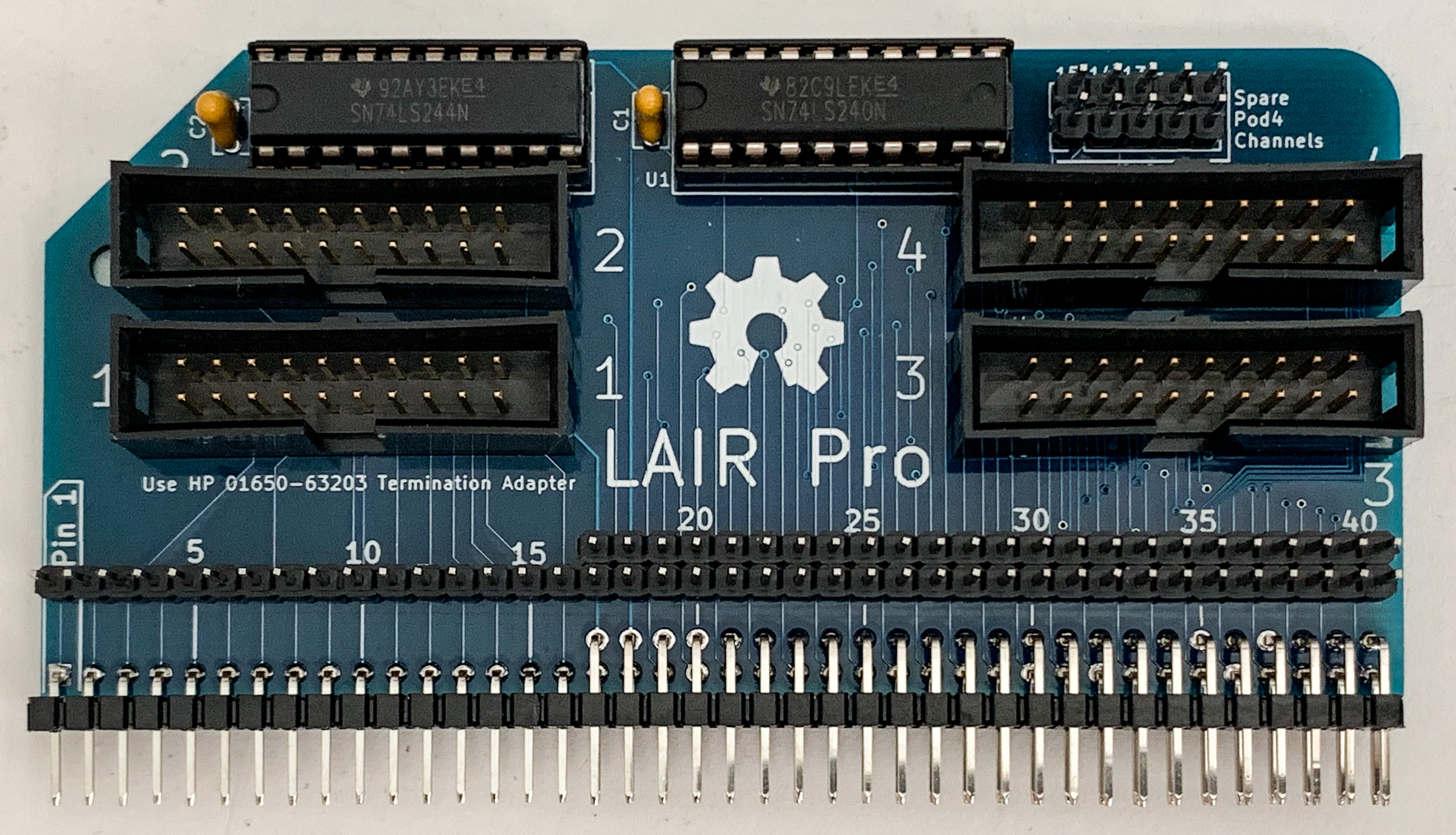
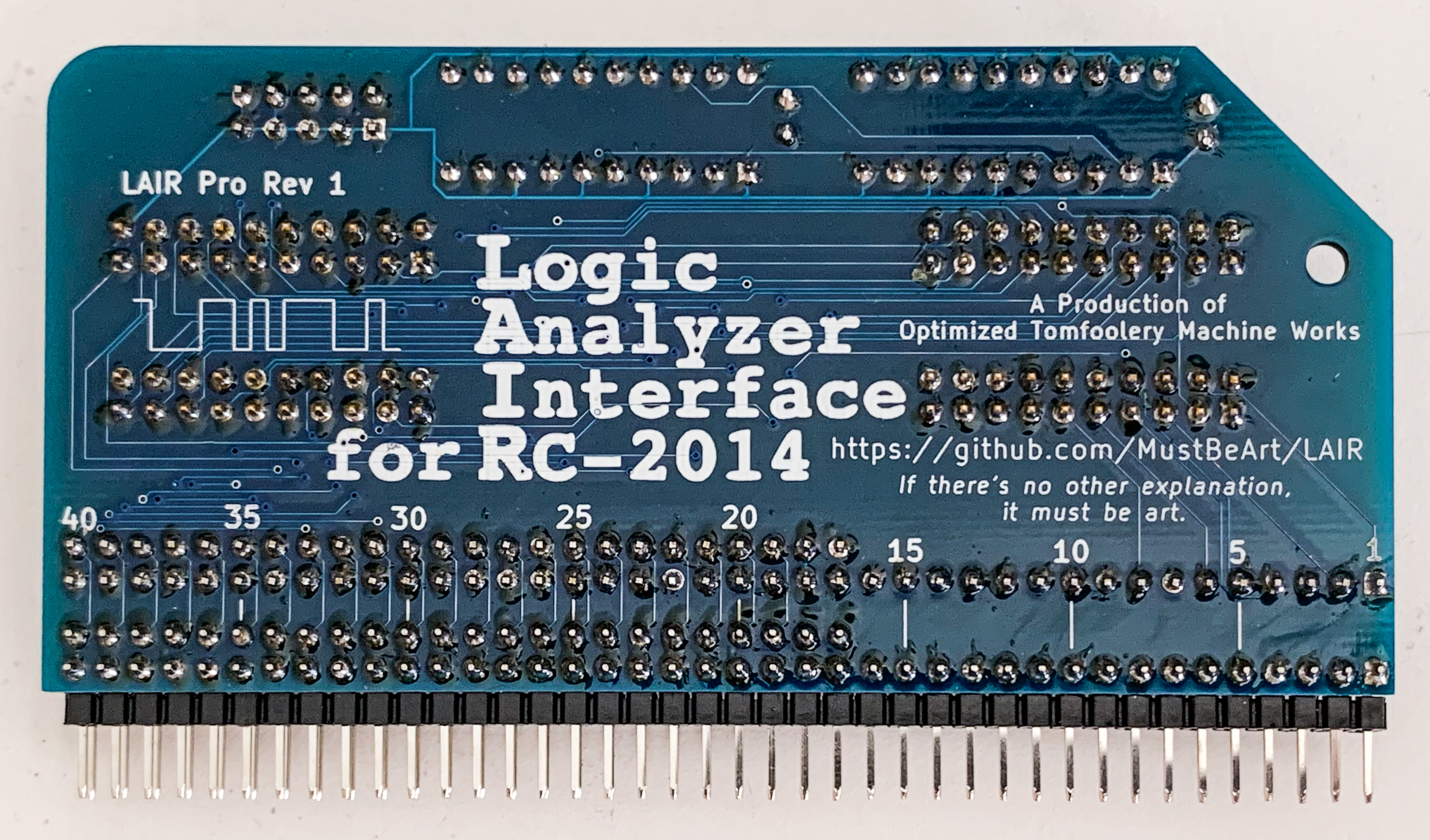
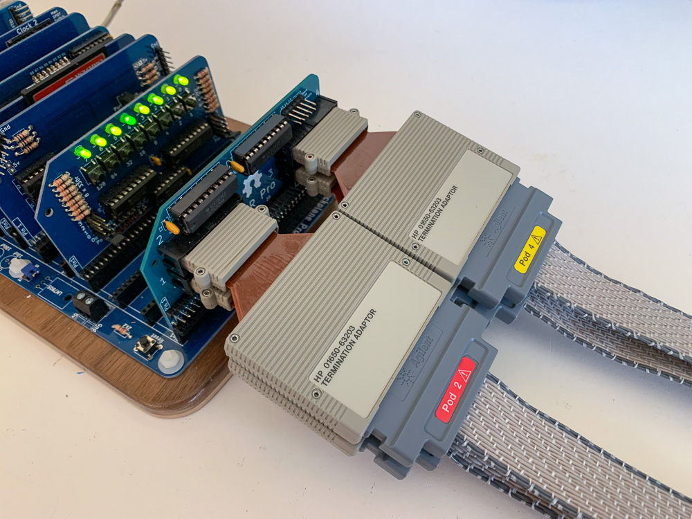
LAIR is an interface that makes it easy to connect a logic analyzer to the backplane bus of a RC-2014 Z80-based retro computer. The logic analyzer can capture all activity on the bus and make it available for analysis, without changing the behavior or timing of the RC-2014 system in any way.
The LAIR module plugs into the RC-2014 Backplane Pro, which includes the standard RC-2014 bus and the enhanced RC-2014 bus. It connects all the pins that are present on the Backplane Pro circuit board. All these pins are also brought out to a second set of pins to make it easy to probe the bus.
The LAIR module is compatible with a range of HP (later Agilent, currently Keysight) logic analyzers from 1984 into the 21st century. The LAIR module has four 20-pin headers designed to be compatible with the HP 01650-63203 Termination Adapter, which terminates the probe cables for these models (and others). Each cable supports 16 channels and one clock signal. LAIR assigns signals to the probe pods in such a way that only two pods are required for basic tracing. With four pods connected, every signal on the bus can be captured, with three channels left over and brought out to a separate connector for use in probing non-bus signals. LAIR Pro was developed and tested on an Agilent 1670G.
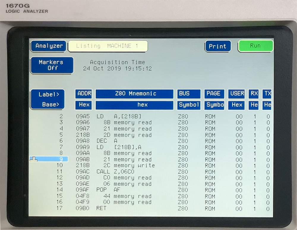
Besides simply wiring up signals from the bus connector to the probe connectors, LAIR has a bit of circuitry to condition the bus signals. This circuitry is modeled after the circuitry used in the HP Model 64683A Interface Module Z80, and makes it easy for the logic analyzer to accurately trace each bus cycle. With the addition of an available "inverse assembler" file, the logic analyzer can capture and display Z80 instruction cycles in standard mnemonic assembler format.
The circuit board was designed using KiCad EDA and all the design files are included (in the hardware directory). The HP1670G directory contains a complete setup for that logic analyzer, including all the RC-2014 bus signals and the HP inverse assembler.
Schematic of Rev 2 LAIR-Pro module (pdf) NOTE: this schematic has not been reduced to a physical circuit board yet. It has only been tested by making modifications to a Rev 1 circuit board, and not comprehensively tested at that.
There are many approaches to debugging programs running on a Z80-based computer such as the RC-2014, but most of them are invasive to some extent. For instance, a debug monitor program can trace execution, but very slowly. Rob Dobson's BusRaider hardware can theoretically trace every bus access made by the Z80, but still at greatly reduced execution speed. Simulation environments like Alan Cox's RC2014 Emulator can trace execution in great detail, not limited by retro hardware speeds, but not on actual hardware. Sometimes there is just no substitute for non-invasive realtime tracing on the actual hardware.
During the CP/M era and beyond, several kinds of solution became available: processor-specific in-circuit emulators, bus analyzers, and general-purpose logic analyzers, each of which had its place. Among them, I'm rather partial to the logic analyzer. It can help solve problems in many kinds of digital systems, not just processor or bus-based systems. I used HP 1630 series logic analyzers to good effect at work in the 1980's and 1990's, and I recently acquired an Agilent (neé HP) 1670G analyzer in pristine condition, thanks to the magic of eBay. These were top of the line professional instruments, designed in the late 1990's. If memory serves, this was the last major revision of HP's original benchtop logic analyzer architecture. This may be stretching the definition of retro a bit out of shape for the CP/M-era purists, but it's old enough for me.
If you were a wealthy company and using a popular processor, you could probably buy a hardware add-on for the logic analyzer that would make it easy to hook up to your target board. In the case of the Z80, that would be HP's Model 64683A Interface Module Z80. These interfaces are very hard to find nowadays, so we need to homebrew an alternative.
There were even software packages you could install on the logic analyzer to disassemble the traced opcodes and present the human-readable assembly language integrated with the trace. Miraculously, these "inverse assembler" packages are available for download even today, including one for the Z80. What's more, HP's 10391B Inverse Assembler Development Package remains available, so you can create your own custom inverse assemblers.
Here's a video on YouTube showing the basic logic analyzer startup procedure:
https://www.youtube.com/watch?v=011vcvdKTC8
HP also made available a Symbol Utility which runs on the logic analyzer and can understand symbols from object files created in several specific object module formats (OMF) that are output by compilers and assemblers. It can also understand a general-purpose ASCII plain text (GPA) format that could be created by hand or by ad hoc tools. The Symbol Utility reads the symbols from these files into a file-based database within the logic analyzer. These symbols are then used in the inverse assembly display and optionally as a column format in the listing view on the logic analyzer's screen.
Even with the inverse assembler and symbol translation, the display on the logic analyzer is fairly primitive. It is also possible to transfer the captured data to a file on an external computer and annotate the traced execution with text from the source code, or from a more sophisticated disassembly listing produced by a reverse engineering tool. The software to do that remains unwritten at this time.
The worst part about using a logic analyzer is hooking up all the individual fiddly wires to all the signals. Getting them all right is difficult, and they are fragile and tend to fall off the target board. You can waste a lot of time chasing down problems that turn out to be errors in the logic analyzer hookup. HP's solution to this problem is to replace the individual probe wires at the end of each ribbon cable with a single connector. It turns out that the probe wires also contain electrical termination of each signal, so the single connector device is called a termination adapter by HP or an isolation adapter by Agilent.
As I write in 2019, the termination adapters are readily available on eBay. The HP 01650-63203 Termination Adapter has a standard 20-pin dual-row female pin header connector, carrying one ground connection, sixteen signal connections, two clock signal connections (though the pods have at most one clock input), and a +5V power output that should not be used. The LAIR Pro has four of the mating shrouded sockets.
Simply plug four termination adapters onto the ends of the ribbon cables for pods 1 through 4, and plug the other end of each termination adapter into the corresponding marked port on the LAIR Pro module. Plug the LAIR Pro module into the RC-2014 Pro Backplane (near one end so there's room for the termination adapters). Load the provided logic analyzer setup file to map all the signals to named labels according to LAIR's scheme. If your logic analyzer is not compatible with the provided setup file, refer to the tables below for signal assignments.
In order to use the inverse assembler, the address bus must be labeled ADDR and the data bus must be labeled DATA. You also need a label STAT that contains (in most-significant to least-significant order) the signals XWR, XIORQ, RFSH, and XM1. The J and K clocks must be connected to MREQ and IORQ, and the L clock must be connected to RFSH. If you're able to use the provided setup file, all this is taken care of for you. The M clock is not used by the inverse assembler or by the standard LAIR Pro setup.
The pin assignments are designed so that you can trace basic bus activity with only pods 1 and 2. However, the inverse assembler depends on the L clock input which appears on pod 3.
The last three signals on pod 4 are not needed for bus signals. They are made available on a separate 10-pin connector in case you need to hook them up to other signals on your RC-2014. The other pins on the 10-pin connector are grounds.
The RC-2014 bus is documented along with the RC-2014 Module Template. Pin 20 on the secondary bus was originally designated for a secondary clock, but it has come to be used for memory paging between ROM and RAM boards, so we will call it PAGE. Note that the signal names used for the RC-2014 bus do not include any indication of polarity, so we have WR and not WR/ or /WR or !WR or WR-with-a-bar-over-it or anything like that, even though WR is an active low signal.
| Pod Signal | RC-2014 Pin | Signal Name | Description |
|---|---|---|---|
| 0 | Main 16 | A0 | Address bus (least significant bit) |
| 1 | Main 15 | A1 | Address bus |
| 2 | Main 14 | A2 | Address bus |
| 3 | Main 13 | A3 | Address bus |
| 4 | Main 12 | A4 | Address bus |
| 5 | Main 11 | A5 | Address bus |
| 6 | Main 10 | A6 | Address bus |
| 7 | Main 9 | A7 | Address bus |
| 8 | Main 8 | A8 | Address bus |
| 9 | Main 7 | A9 | Address bus |
| 10 | Main 6 | A10 | Address bus |
| 11 | Main 5 | A11 | Address bus |
| 12 | Main 4 | A12 | Address bus |
| 13 | Main 3 | A13 | Address bus |
| 14 | Main 2 | A14 | Address bus |
| 15 | Main 1 | A15 | Address bus (most significant bit) |
| J CLOCK | Main 23 | MREQ | Z80 MREQ, memory request |
Rising edges on the J clock input on Pod 1 are used to detect memory bus cycles.
| Pod Signal | RC-2014 Pin | Signal Name | Description |
|---|---|---|---|
| 0 | Main 27 | D0 | Data bus (least significant bit) |
| 1 | Main 28 | D1 | Data bus |
| 2 | Main 29 | D2 | Data bus |
| 3 | Main 30 | D3 | Data bus |
| 4 | Main 31 | D4 | Data bus |
| 5 | Main 32 | D5 | Data bus |
| 6 | Main 33 | D6 | Data bus |
| 7 | Main 34 | D7 | Data bus (most significant bit) |
| 8 | N/A | XWR | Delayed, inverted version of Z80 WR |
| 9 | N/A | XIORQ | Delayed version of Z80 IORQ |
| 10 | Enh 19 | RFSH | Z80 RFSH, refresh request |
| 11 | N/A | XM1 | Delayed version of Z80 M1 |
| 12 | Main 25 | RD | Z80 RD, read enable |
| 13 | Main 23 | MREQ | Z80 MREQ, memory request |
| 14 | Main 22 | INT | Z80 INT, interrupt request |
| 15 | Main 20 | RESET | Z80 RESET |
| K CLOCK | Main 26 | IORQ | Z80 IORQ, input/output request |
Rising edges on the K clock input on Pod 2 are used to detect I/O bus cycles, including interrupt acknowledgement cycles.
| Pod Signal | RC-2014 Pin | Signal Name | Description |
|---|---|---|---|
| 0 | Enh 26 | NMI | Z80 NMI, non-maskable interrupt |
| 1 | Enh 25 | WAIT | Z80 WAIT, wait state request |
| 2 | Enh 24 | BUSRQ | Z80 BUSRQ, bus release request |
| 3 | Enh 23 | HALT | Z80 HALT, stop processor |
| 4 | Enh 22 | BUSACK | Z80 BUSACK, bus release acknowledge |
| 5 | Enh 21 | CLOCK2 | Secondary clock |
| 6 | Enh 20 | PAGE | Paging from ROM to RAM (aka RESET2) |
| 7 | Main 24 | WR | Z80 WR, write enable (not delayed) |
| 8 | Main 37 | USER1 | reserved for user functions |
| 9 | Main 38 | USER2 | reserved for user functions |
| 10 | Main 39 | USER3 | reserved for user functions |
| 11 | Main 40 | USER4 | reserved for user functions |
| 12 | Enh 37 | USER5 | reserved for user functions |
| 13 | Enh 38 | USER6 | reserved for user functions |
| 14 | Enh 39 | USER7 | reserved for user functions |
| 15 | Enh 40 | USER8 | reserved for user functions |
| L CLOCK | N/A | RFSH | Z80 RFSH, refresh request |
Pod 3's L clock signal is used as a clock inhibit to prevent DRAM refresh cycles from being logged.
| Pod Signal | RC-2014 Pin | Signal Name | Description |
|---|---|---|---|
| 0 | Enh 34 | D8 | 16-bit data bus |
| 1 | Enh 33 | D9 | 16-bit data bus |
| 2 | Enh 32 | D10 | 16-bit data bus |
| 3 | Enh 31 | D11 | 16-bit data bus |
| 4 | Enh 30 | D12 | 16-bit data bus |
| 5 | Enh 29 | D13 | 16-bit data bus |
| 6 | Enh 28 | D14 | 16-bit data bus |
| 7 | Enh 27 | D15 | 16-bit data bus (most significant bit) |
| 8 | Main 36 | RX | serial data receive (input to RC-2014) |
| 9 | Main 35 | TX | serial data transmit (output from RC-2014) |
| 10 | Enh 36 | RX2 | second serial data receive |
| 11 | Enh 35 | TX2 | second serial data transmit |
| 12 | Main 26 | IORQ | Z80 IORQ, input/output request (not delayed) |
| 13 | N/A | Spare 13 | spare logic analyzer channel |
| 14 | N/A | Spare 14 | spare logic analyzer channel |
| 15 | N/A | Spare 15 | spare logic analyzer channel |
| M CLOCK | Main 21 | CLOCK | Z80 CLOCK, main system clock |
Pod 4's M clock signal is not used by the standard LAIR Pro logic analyzer configuration, but is connected to the main system clock to enable custom configurations.
The three spare inputs appear on their own connector in case you want to use them.
There are now some inexpensive but powerful logic analyzers based on FGPA technology, such as the Logic and Logic Pro line from Saleae (and clones thereof), or any of the commercial and DIY units compatible with the open-source sigrok signal analysis software suite. These are extremely useful devices for the retro computer enthusiast, but they are not capable of tracing the RC-2014 bus the same way the LAIR Pro does with an HP/Agilent analyzer. There are two main reasons.
The simple reason is that none of these modern products has enough channels. Saleae tops out at 16 channels, and the widest unit listed on sigrok's Supported Hardware page is 34 channels. A basic trace of bus cycles requires 16 address bits, 8 data bits, and 4 conditioned bus control signals, so a 32-bit analyzer might suffice, but the more common 16-bit models are insufficient. It would take a 64-bit analyzer to capture every signal on the bus, as the LAIR Pro does.
The other reason has to do with what type of logic analyzer we need. All of these modern devices, as far as I know, are what HP calls timing analyzers, which means that they sample the data based on a free-running clock generated within the analyzer. The LAIR Pro uses the state analyzer function of the supported logic analyzers. That means it samples the data based on clocks derived from the system under test, the RC-2014 in our case.
With a state analyzer, we can capture exactly one sample for each bus cycle, which is what we need. In order to capture the same information with a timing analyzer, we would need to run the freerunning clock at some multiple of the system clock, which is a bigger multiple of the bus cycle rate. The higher sample rate would generate correspondingly more data, filling up memory faster, and also generates data that isn't nearly as easy to understand. You'd probably want to run a post-processor on the sample data to find the bus cycles and re-create the kind of trace we get directly from a state analyzer.
On the other hand, the modern analyzers have a huge advantage in memory capacity. The vintage HP analyzers store state data to internal memory, where they have room for anywhere from 64K samples to 2M samples (and higher for more recent models). Many of the modern analyzers stream in real time over USB to a modern computer, where storage is practically unlimited by comparison. Even the ones that store to local memory have far more memory than the vintage analyzers do. So, until we hit the streaming bandwidth limit, the extra load of data generated by the timing analyzer is not really a problem.
That leaves the need for a post-processor to help us understand the results in terms of bus cycles. That is a small matter of programming, but not insurmountable. Perhaps a project for a future day.
One thing the post processor can't help with is triggering. Since the state analyzer is aware of bus cycles in real time, it's easy to set up the analyzer to detect various code execution scenarios in all sorts of flexible ways, and use that to begin, end, and filter our data capturing. The timing analyzers generally have less flexible triggering capabilities. Some smart triggering would still be possible, but it would be messier and probably less flexible on a timing analyzer.
I'm sure they're great. Keysight's cheapest current model with enough channels starts at $20,000. And it's not retro, yet.
The Z80 bus has lots of signals for bus management, including some redundancy to make it relatively easy to implement peripheral devices. The most essential of those signals (for a minimal Z80 system) are included in the standard bus on the RC-2014. Other signals for more advanced systems were added with the enhanced bus on the RC-2014 Pro.
All bus cycles involve either MREQ (memory request) or IORQ (input/output request). MREQ is active for reads and writes to memory, including opcode fetches and DRAM refreshes. IORQ is active for reads of input ports and writes of output ports, and also for interrupt acknowledgement cycles. As a result, we can capture all these bus cycles by looking for active pulses on MREQ and IORQ.
In order to distinguish the types of bus cycles, we have RD, WR, M1, RFSH.
When found with MREQ, RD is active for memory reads, including opcode fetches and DRAM refreshes. WR is active only for memory writes. M1 is active only for opcode fetches. RFSH is active only for DRAM refreshes. So, we can ignore the RD signal and rely on WR, M1, and RFSH to decode exactly what kind of MREQ cycle we have.
When found with IOREQ, RD is active for input reads and interrupt acknowledges. WR is active only for output writes. M1 is active only for interrupt acknowledges. So we can again ignore RD and rely on WR and M1 to decode the IORQ cycle type.
The obvious implementation of this understanding is to clock the logic state analyzer on the trailing edges of MREQ and IORQ, and decode WR, M1, and RFSH to determine what kind of bus cycle we've captured. That is indeed what we do, but we have to pay attention to the details of Z80 bus timing to make it work. Fortunately, the HP engineers who designed the Model 64683A Interface Module Z80 have shown us the way.
Ideally, we would follow their lead exactly, so as to achieve the same performance guarantees and to maintain complete compatibility with their inverse assembler. The HP designers conservatively chose to buffer every monitored signal. We can't do the same with a standard RC-2014 modules size and through-hole components. We will play a little fast and loose with signal quality concerns and connect directly to the bus signals. This changes the timing of everything by one gate delay.
HP's adapter ran MREQ and IORQ through an inverter and used both of them to clock the state analyzer. We can't do the same, since the other signals aren't delayed. We use MREQ and IORQ directly as J and K clock inputs. This doesn't hurt compatibility with the inverse assembler, but it does mean that the logic analyzer's Master Clock has to be configured to detect rising edges on J or K instead of falling edges.
The WR signal is not valid at those edges. HP's adapter corrects this problem by running WR through three inverters. We need one fewer gate delay, so we use one inverter and one non-inverting buffer. Likewise, M1 is not quite valid at those edges. HP's adapter, at least according to the description I received, does not address this issue, but we add a non-inverting buffer.
The analyzer is being clocked by both MREQ and IORQ, but it does not automatically keep track of which clock source latched a particular state. In order to find out, we have to delay the clock source (so it remains valid through the transition) and capture it as a state input. HP's adapter runs IORQ through two inverters. We need one fewer gate delay, so we use one non-inverting buffer. We don't need a delayed version of MREQ, because if the state capture wasn't clocked by IORQ, we know it was clocked by MREQ.
For most debug purposes, we don't care to see DRAM refresh cycles. Unless there's a fundamental hardware problem, the DRAM refresh doesn't have anything to do with the flow of program execution. It would be ideal if we could just discard those cycles without storing them. In order to do that on the HP logic analyzer, we need to use a clock qualifying input, and the only signals that can qualify the clocks are other clock inputs. So we connect RFSH to the third clock input L. If we program the analyzer's clock to react to J (MREQ) or K only if L is not active, we don't capture DRAM refresh cycles. If we turn off L as a clock qualifier, we do capture DRAM refresh cycles, and we can recognize them because we also have RFSH as a captured signal.
That leaves us with a spare clock input M. We don't need it for the inverse assembler. LAIR connects the system clock to M for possible use in debugging bus cycle timing or operation of peripheral devices that use the system clock. Unfortunately, we don't have a spare clock input for the CLOCK2 secondary clock signal on the enhanced RC-2014 bus.
If possible, use the configuration file (lair_v1._a) provided with LAIR Pro. This file is known to work with my Agilent 1670G analyzer. If your analyzer is different, try it anyway and see what happens.
You'll need to transfer two files into your logic analyzer. lair_v1._a is the configuration file, and iz80_i is the HP inverse assembler program for Z80. If your logic analyzer has an Ethernet connection to your network, you can transfer these files by FTP. Or, if you have a computer with a 3.5" floppy disk drive, you can copy them onto a floppy and then use the logic analyzer's front panel controls to copy them from the floppy onto the logic analyzer's hard drive.
Then use the logic analyzer's front panel controls to LOAD the configuration from lair_v1._a.
If you can't load the configuration from lair_v1._a, you can enter the configuration manually. Here is a dump of the logic analyzer configuration and some screenshots of the logic analyzer configuration you can refer to. Once you get the analyzer configured correctly, save your configuration to a file so you can use it again next time.
(links in previous paragraph not active yet)
Unfortunately, there's no way to enter the inverse assembler manually. You'll have to get one of the file transfer methods working in order to use it.
After you load the configuration (either lair_v1._a or one you created), check the listing screen and see if the DATA column has been replaced by an inverse assembler column. If not, you'll need to load the inverse assembler manually. Go back to the Hard Drive screen and LOAD to the ANALYZER from the file iz80_i. Check the listing screen again; it should now be displaying the inverse assembler. If you now save your configuration, the inverse assembler should load automatically next time.
LAIR Pro is designed for use with the Pro Backplane. Plug LAIR Pro into a slot that has the Enhanced Bus connector installed.
The Pro Backplane kit ships with enough 40-pin female headers to populate the Standard Bus on every slot. However, it only ships with a limited number of female headers for the Enhanced Bus, and those connectors are only 20 pins long, which doesn't give access to the four USER pins on the Enhanced Bus connector. You can add Enhanced Bus connectors to the slots that have none, and I suggest you use 24-pin headers. Then you'll need to arrange to have all the modules that use the Enhanced Bus USER pins plugged into these fully populated slots. That includes the LAIR Pro, if you wish to trace the Enhanced Bus USER pins on the logic analyzer.
If you want to go back and add the USER pins to the slots that already have 20-pin connectors on the Enhanced Bus, you'll run into a problem. You can't add female headers next to existing female headers without skipping a pin, because the plastic housings collide. If you're comfortable desoldering, you can remove the existing 20-pin female headers and install new 24-pin ones. That's what I did.
If your RC-2014 doesn't support the Enhanced Bus from the RC-2014 Backplane Pro, you can still use LAIR Pro. If you don't need to use the inverse assembler, no special steps are necessary. Of course, you won't see any information on any of the signals from the Enhanced Bus.
In order to run the inverse assembler, you'll need to hook up the RFSH signal. Use the regular individual wires connector on Pod 3 (not the termination adapter). Connect the ground wire to a convenient ground on your RC-2014. Connect the L clock wire to the RFSH signal on your Z80. If your Z80 CPU board has the Enhanced Bus, you can clip onto pin 19 on the Enhanced Bus connector. Otherwise, you can clip directly onto the RFSH/ signal right on the Z80 chip (pin 28 on the usual DIP package).
If you've already built your RC-2014, assembling the LAIR-Pro will present few new mysteries.
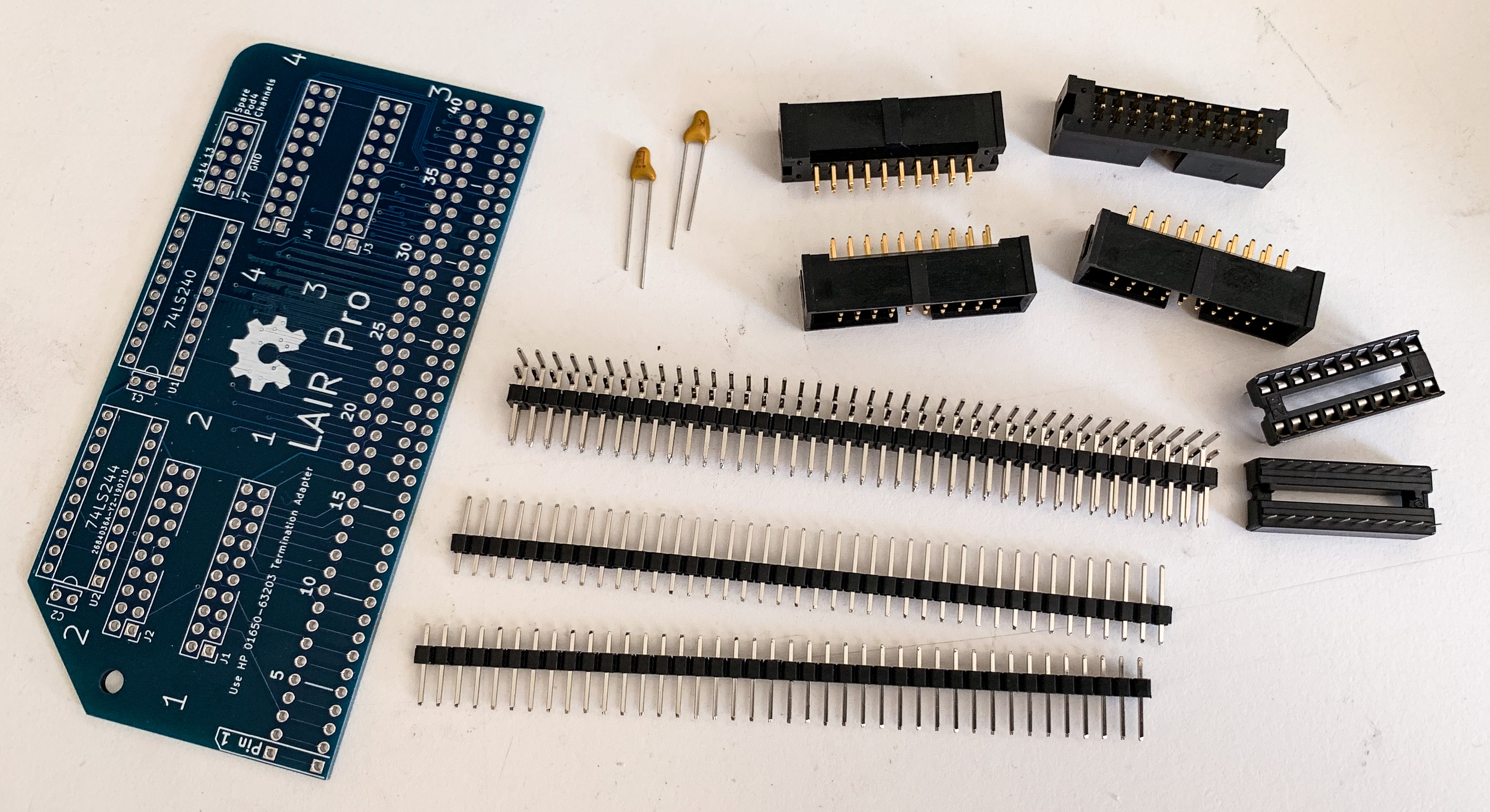
LAIR Pro has two sets of holes for the RC-2014 Pro bus. Install the usual right-angle dual-row header at the bottom, nearest the edge of the board. The other set of holes is right above that, and is intended to make it easier to connect random probe wires to bus signals. Install straight headers in that set of holes. You can use dual-row male headers or two single-row headers. If you don't think you'll ever want to use these headers for probing, it's perfectly OK to leave them out.
See Preparing Enhanced Bus Connectors for good advice on installing the right-angle bus connector. Go ahead and remove the first 16 pins as suggested, but don't remove any pins from the other end; LAIR Pro even has room for pin 40.
The Agilent manual for the Isolation Adapter specifies part numbers from Agilent and from 3M for the mating connector. These part numbers are so obsolete I wasn't even able to find specifications on them. However, the part required is a perfectly ordinary 20-pin dual-row shrouded male header (thank you, HP engineers). I ordered Samtec TST-110-01-G-D (catalog page) and they work fine. Any other vendor's similar connector would probably work, too. I don't recommend using unshrouded male headers, though they would work. The shrouds help support the weight of the termination adapter and pod cables, and they make it impossible to plug them in backwards or off-by-one.
If you want a LAIR Pro right now, you'll have to build it from scratch. You can start with the Rev 2 design files in the hardware directory, output Gerbers, and order from your favorite PCB manufacturer. Then you'll have to find the connectors and other parts. You can do it! If you have never had a board made before, you'll find the experience educational.
If there is interest from the community, I can put together LAIR Pro kits. Please let me know if you are interested in a LAIR Pro kit.
