
###Part_Style_Guide
Part Style Guide for part footprints.
This document dictates how parts are designed and styled to give a consistent experience for users and increase the speed of the pick and place vision systems.
All documentation and examples can be found on the GitHub repository.
Eagle V6+
Eagle’s parts are broken down into 3 levels: Footprints which are the PCB level, Symbols which are the Schematic level, and Devices which is how the Footprints and Symbols connect to each other. Each Footprint, Symbol, and Device belong to an over arching library to organize the parts.
Libraries
Each part will be pre-classified to which library it will be added to. The list of these are as follows.
- MF_Sensors
- MF_PowerIC
- MF_Passives
- MF_LED
- MF_FreqCtrl
- MF_Electromechanical
- MF_Displays
- MF_DiscreteSemi
- MF_DigitalIC
- MF_Connectors
- MF_AnalogIC
- MF_Aesthetics
Footprints
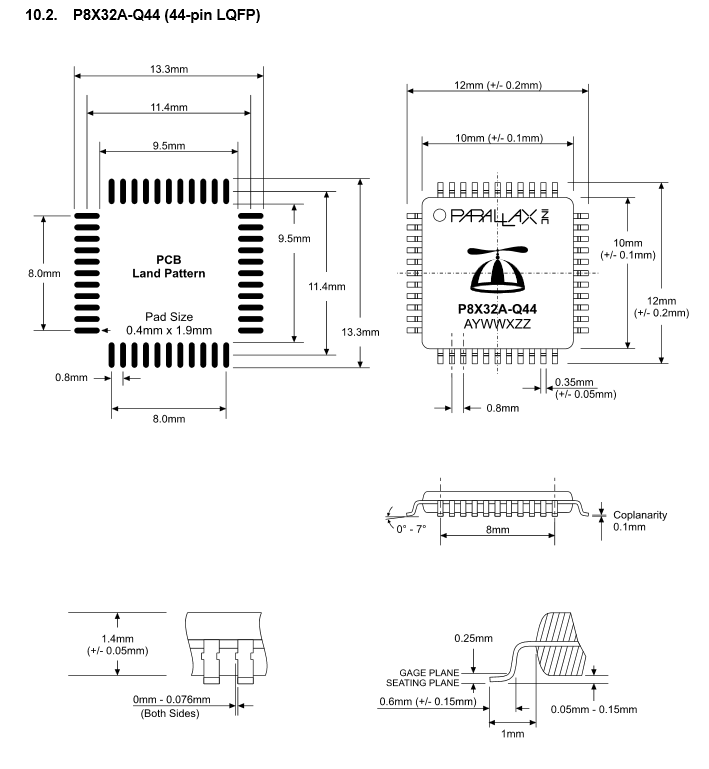
Footprints are defined as the physical representation of the part on a PCB. The name of the footprint should be listed in the datasheet of the part. The convention to be used will be no hyphens or underscores.
Example: SSOP-28 would be named SSOP28
Use the Manufacturer's specific layout/package for the footprint if it is in the part’s datasheet. Otherwise, use the following guidelines.
-
Pad size should be determined by the nominal width of the lead and double the length of the landing area of the pad.
-
Pitch of the leads shall be determined by the nominal width of the lead.
-
Center of the pads will be at the max width of the leads.
-
Center of the footprint shall be the origin.
-
Pin 1 of the footprint will start in the upper left side of the footprint and count down.
-
Each footprint will be enclosed by a silkscreen. This silkscreen must represent the maximal area of the part and enclose the pads. The thickness of this silkscreen is 0.127mm or 5mils.
-
Orientation of the footprint will be denoted with a filled in rectangle and be near pin 1.
-
Pads will be named by the normal naming convention of Eagle. Ex. P$1, P$2….
-
Each footprint will have the designator near the first pin of the footprint. The specifications for the designator are as follows.
- Size: 1.016mm or 40mils
- Ratio: 16%
- Line Distance: 50%
- Font: Vector
- Layer: 25 tNames
- Value: >NAME
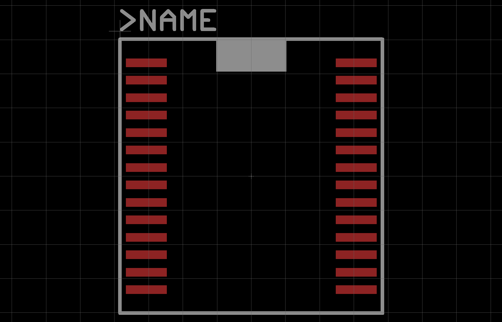
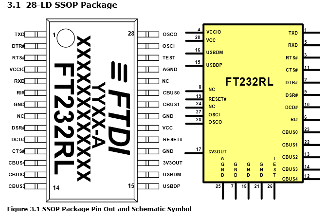
Example: FT232RL in SSOP-28

The package dimensions for the FT232RL can be found on page 35 of the datasheet.Package name would be SSOP28. Pad size would be .3mm x 1.5mm. Pitch would be .65mm. Centers of the pads would be 7.8mm apart from each other.
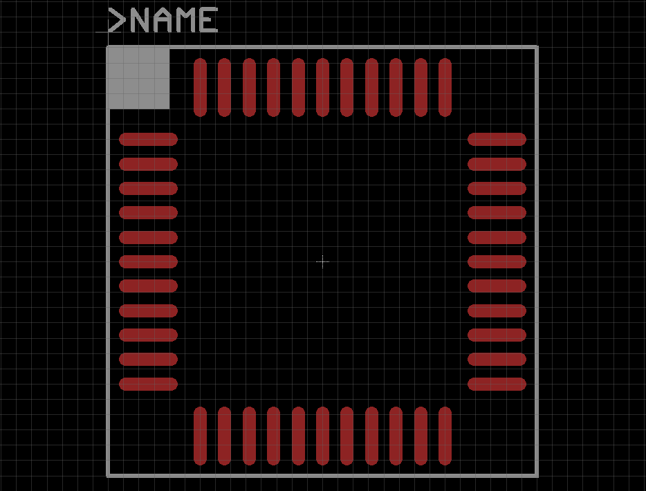
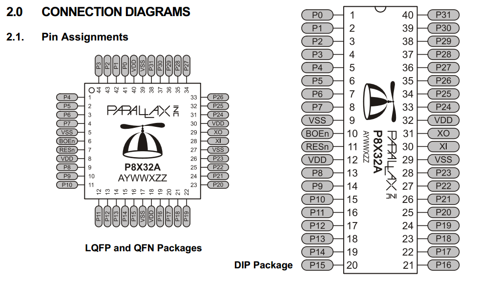
Example: P8X32-Q44
The package dimensions for the P8X32-Q44 can be found on page 34 of the datasheet. Parallax defines a set PCB Land Pattern so that will be used. Package name would be LQFP44. Pad size would be .4mm x 1.9mm. Pitch would be .8mm. Centers of the pads would be 11.4mm apart from each other.
Symbols
Symbols are defined as the schematic representation of the part. The name of the symbol should be the family name of the part.
Example: FT232RL will be called FT232R as that is the family name of the part.
Use the Manufacturer's datasheet of the part to build the symbol. Usually included in the datasheet are appnotes and schematic symbols that should be used in designing the symbol.
1. Digital grounds will be represented by one pin. Same goes for Power and Analog grounds. Gounds shall be named GND and Power shall be named VCC.
2. NC or No Connection should not be included in symbol.
3. Use a “!” at the beginning of the pin name to denote active low states.
4. Center the symbol around the origin.
5. Rectangle to represent the part will be width 10mils and on layer “94 Symbols”.
6. Name and Value of the symbol will be near the top left corner. Font will be size 40mils, ratio 8%, font vector. >NAME will be placed in the “95 Names” layer and >VALUE will be placed in “96 Values” layer.
7. A detailed description of the part is required. Showing what the family part number is, manufacturer, and a short description of the part. The description field uses standard HTML formatting. Use the following example as a template.
<b>Manufacturer Part #:</b> FT232R<br/>
<b>Manufacturer:</b> FTDI<br/>
<b>Description:</b> USB Interface IC USB to Serial UART IC<br/>
<b>Datasheet:</b> <a href="http://www.ftdichip.com/Support/Documents/DataSheets/ICs/DS_FT232R.pdf">Link</a>
8. Each pin must have the direction set. The direction of the pin should be set using the following guidelines.
- In: input
- Out: output
- IO: in/output (bidirectional)
- OC: open collector or open drain
- Hiz: high impedance output (3-state)
- Pas: passive (resistors, capacitors, inductors)
- Pwr: power input pin (Vcc, Gnd, Vss, Vdd)
- Sup: general supply pin (ground symbol) Do not use on part symbols.
9. Other pin properties are as follows
- Name: Use Name of the Pin
- Length: short
- Function: none
- Visible: pin
Example: FT232R

Example: P8X32

Devices
Devices are defined as the way the symbol and footprint connect to each other. The name of the device should be the family name of the part.
Example: FT232RL will be called FT232R as that is the family name of the part.
-
Value is turned “on”
-
Name of package variant should be the name of the package.
-
Combine Ground pins and Power pins if applicable.
-
Description should follow the Symbols template.
-
Prefixs for the devices are shown below
- C - capacitor
- D - diode/LED
- J - header pins or connectors
- JP - jumper
- L - inductor
- Q - transistor/FET
- R - resistor
- SW - switch
- TP - test point
- U - integrated circuit (sensor, MCU, etc.)
- X - crystal or oscillator
- The following attributes should be added to each device.
- HOUSEPART
- MPN
- POPULATE
- URL
- VALUE
See MF_Examples.lbr for all the examples.