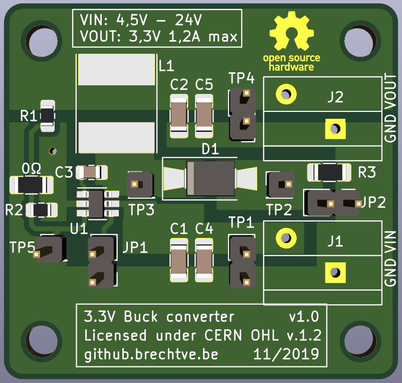
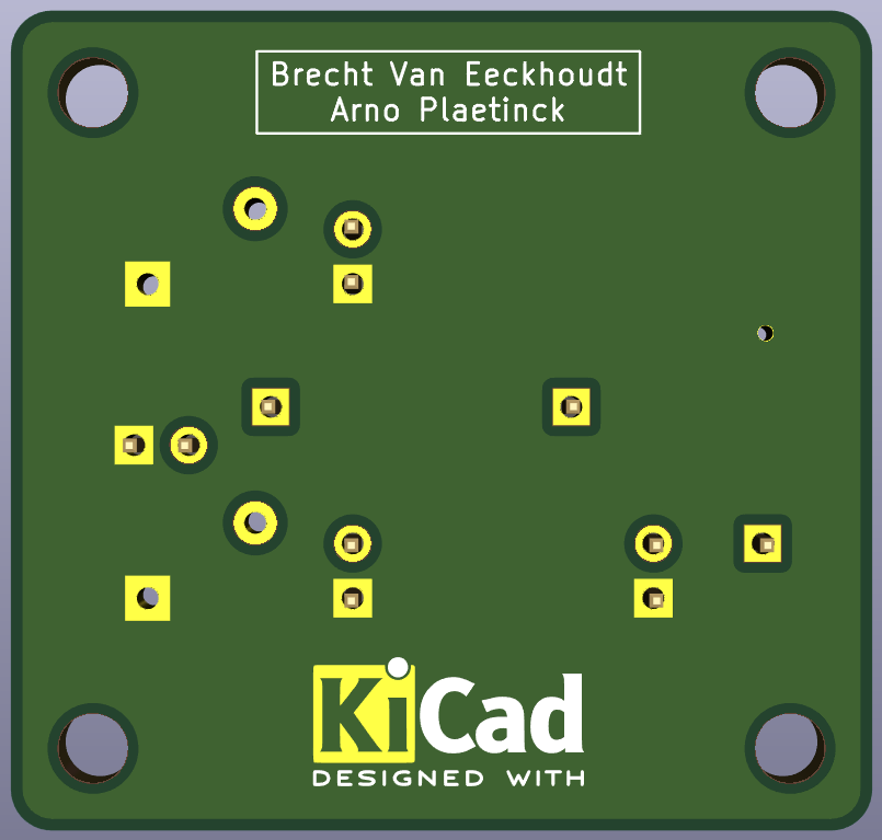
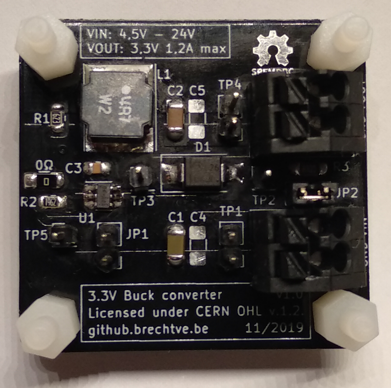
The goal of this lab was to design a 5 - 9V to 3,3V (500 mA min) buck converter from the ground up. We had to start from a given chip (RT8259GE) and create the rest ourselves.
Careful layout considerations were taken to lead to an optimal design. The 0Ω resistor is not on the schematic but only on the board layout. It's footprint was used to jump over the feedback track so everything is on the top layer. A via to GND is placed around it as well for redundancy.
JP1can be used to disable the buck converter.JP2can be used to bypass the sense resistorR3(measures the diode current).- A lot of test points (
TPx) are given to be able to measure different voltages. C4andC5are footprints for extra capacitors if the signals have too much ripple.
- VIN: 4,5 - 24 V
- VOUT: 3,3 V @ 1,2 A max
| Component | Value | Footprint | Other | Ordering |
|---|---|---|---|---|
| U1 | RT8259GE | SOT-23-6 | Richtek | |
| C1, C4 | 10 µF | 1206 | (X7R), 50V, 10% | Mouser.be |
| C2, C5 | 22 µF | 1206 | X7R, 10V, 10% | Mouser.be |
| C3 | 10 nF = 0,01 µF | 0805 | X7R, 50V, 10% | Mouser.be |
| D1 | If = 2A Vr = 40V Vf = 0,43V | SMA/SMB | Mouser.be | |
| L1 | 4,7 µH | NR8040 | Taiyo Yuden | Mouser.be |
| R1 | 62 kΩ | 0805 | 0,5% | Mouser.be |
| R2 | 19,6 kΩ | 0805 | 0,5% | Mouser.be |
| R3 | 0,1 Ω = 100 mΩ | 1206 | 1% | Mouser.be |
| 0Ω | 0 Ω | 1206 | Mouser.be | |
| J1, J2 | PTSA_1,5/_2-3,5-Z_BK | Pitch: 3,5 mm | 2 contacts, 250V 2A | Mouser.be |
WARNING: The pinout of J1 and J2 is reversed due to a footprint error (wrong top/bottom view). The Phoenix Contact connectors can however be manually separated and put back together in a way that they do fit on the board.


