Xilinx Project for MIPS Pipeline CPU with 5 stages
This is a repository maintained for Computer Architecture Studies
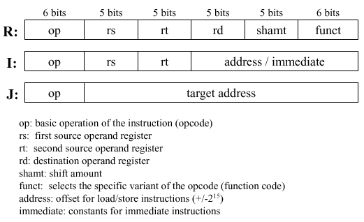
The MIPS CPU supports MIPS-C4 Instruction Set
MIPS-C4 = {LB、LBU、LH、LHU、LW、SB、SH、SW、ADD、ADDU、SUB、SUBU、MULT、MULTU、DIV、DIVU、SLL、SRL、SRA、SLLV、SRLV、SRAV、AND、OR、XOR、NOR、ADDI、ADDIU、ANDI、ORI、XORI、LUI、SLT、SLTI、SLTIU、SLTU、BEQ、BNE、BLEZ、BGTZ、BLTZ、BGEZ、J、JAL、JALR、JR、MFHI、MFLO、MTHI、MTLO、ERET、MFC0、MTC0}
| Project | Feature | Folder |
|---|---|---|
| 1 | Supports MIPS-C4 ISA | Basic CPU |
| 2 | Adds Pause and Interrupt | Standard CPU |
| 3 | Supports MIPS Microsystems | Advanced CPU |
Full Instruction Document for MIPS32
Designed to be Five-stage Pipeline
- Fetch Instruction at F-Stage
- Access Register Files at D-Stage
- Do Arithmatic at E-Stage
- Access Memory and Devices at M-Stage
- Write Back to Register File at W-Stage
In MIPS System, Hazards can be properly handled
Stall and Forward can break the data hazard while bring the Compare Unit forward to D-Stage can solve the control hazard
When designing the system, two coding styles stand out
Detector
Only detect the potential hazards
When detected, do the necessary operations
Planner
List all possible conflicts and handle each one of them properly in advance
Personally, I prefer Detector Coding Style to Planner Coding Style
Adds CoProcessor 0 which handles Pauses and Interrupts
- Pause
Pause will arise from outside devices such as Timers
When Pause signal arrives, CP0 Processor will hold & clear the pipeline until Exception Handler Code arrives
Memory Mapping
| Address | Function | R/W |
|---|---|---|
| 0x00000000-0x00003000 | Data Memory | R W |
| 0x00003000-0x00004fff | Instruction Memory | R |
| 0x00004fff-0x0000xxxx | Device Space | R W? |
- Interrupt Interrupt can be caused by Exceptions inside CPU
| ExcCode | Symbol | Description |
|---|---|---|
| 0 | INT | Interrupts |
| 4 | AdEL | Fetch Error |
| 5 | AdES | Store Error |
| 10 | RI | Unrecognized Op Code |
| 12 | OV | Arithmatic Overflow |
In this project, I introduced MIPS Microsystem into the project
Devices are mapped as below
| Address | Device |
|---|---|
| 0x00007f00-0x00007f0b | Timer |
| 0x00007f10-0x00007f2b | MiniUART |
| 0x00007f2c-0x00007f33 | 64-bit Switch |
| 0x00007f34-0x00007f37 | 32-bit LED |
| 0x00007f38-0x00007f3f | Digital Tube |
| 0x00007f40-0x00007f43 | 8-bit Button |
Because I need to burn the .bit file into FPGA board, the whole system must be Synthesizable
Use IP Core instead of instantiate reg files can speed up the synthesize process
Also, a bridge is needed to handle the communication between CPU and Devices


