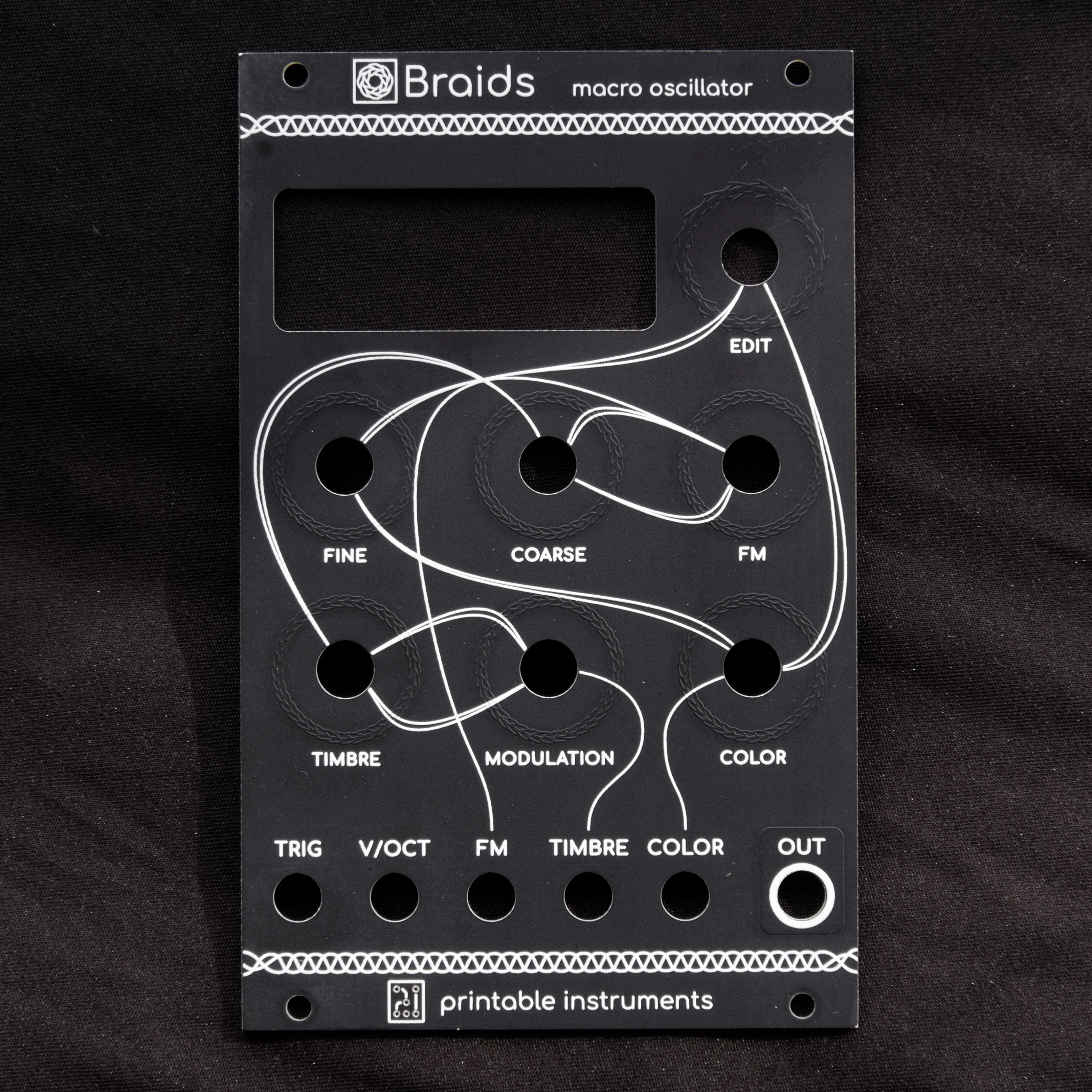
The Printable Instruments project provides custom PCB panel designs for Mutable Instruments modules. These panels are meant to be ordered from PCB manufacturers such as PCBWay or JLCPCB.
All the panels are created using Inkscape. The Inkscape extension svg2shenzhen is used to generate a KiCad project from the Inkscape svg, which can then be used to generate gerber files.
Additionally to the Printable Instruments panel designs, this repository also contains panel templates, which can be used to easily create your own designs.
The development of the Braids panel and the 2.0 release of this project was generously sponsored by PCBWay, who provided free samples of the Braids panel!
- Rings
- Clouds
- Ripples (2015)
- Blinds
- Veils (2016)
- Frames
- Links
- Marbles
- Braids
Warning: Unchecked panels are still in development and haven't been ordered/tested yet!
-
Mutable Instruments provided the original hardware design files, which are being used as references in this repository.
-
The Mutated Mutables repository has been very helpful for figuring out the Inkscape to KiCad workflow. Some graphics from the "Doku" layer have been directly adopted in this repository.
- angiamusic made a really nice Frames panel based on this project
Note: for v2.0+ there's pregenerated gerber files in the latest release.
You can simply download the printable-instruments-gerbers.zip, unpack it and upload any of
the contained gerber archives to your favorite board house.
-
Install Inkscape, KiCad.
-
Install the svg2shenzhen extension, according to the installation instructions.
-
Open a svg panel file in Inkscape.
-
(optional) When ordering from a different service than JLC, change the "JLCJLCJLCJLC" text, to whatever your manufacturer is using as a template for order numbers. Some manufacturers also have options to completely remove the number for a small premium. You most certainly don't want the order number on the front of your panel.
-
In Inkscape: Extensions -> Svg2Shenzhen -> 2. Export to KiCad...
Recommended settings:
Export As Project Threshold Default (5) Export DPI Default (1200) Flatten Bezier yes Open Kicad yes Click Apply
-
By default, all the holes from the Drill layers will be plated through holes, which will leave a small, visible ring of copper exposed. To fix this, I'd recommend manually going through all the holes, except the small vias from the bottom logo (because for those, the effect is actually wanted) in Pcbnew and changing their pad type to "NPTH, Mechanical".
-
In Pcbnew: File -> Plot...
Recommended settings:
Plot format Gerber Included Layers F.Cu, B.Cu, F.SilkS, B.SilkS, F.Mask, B.Mask, Edge.Cuts Click Plot
-
Click Generate Drill Files... (still in the Plot window)
Recommended settings:
Map File Format Gerber Drill Units Millimeters Click Generate Drill File
-
I wasn't completely happy with this first version design wise, mainly because many of the module icon designs where copied from the original MI panel designs. The icons which weren't also had some consistency issues which I tried to resolve.
They also had some visible flaws when I first ordered them from JLCPCB. Many of the (cheaper) PCB Manufacturers seem to have a problem with filled silkscreen areas, where the silkscreen doesn't fully cover up the solder mask. Sometimes there are also visible lines in those areas. Because of that all the filled areas got removed.


